ESP32 Dev Board vs Custom PCB: When to Switch
Every ESP32 product starts on a dev board. That is the right way to start — you get a working

Everyone talks about PCB layout, but the schematic is where most of the expensive mistakes actually happen. A layout error costs you a respin; a schematic error costs you a respin *and* the time you spent laying out a board that was never going to work.
This guide covers esp32 schematic design that survives translation into hardware, and the review process that catches problems before layout begins.
An esp32 schematic diagram is a contract between several parties: you, the layout engineer, the firmware team, and the manufacturer. If anything in it is ambiguous or wrong, one of them will pay for it.
A good schematic is therefore:
The goal is not a pretty drawing; it is a drawing that leaves no room for interpretation. A reviewer should be able to open the file and understand the intent without a phone call.
Espressif publishes reference schematics for each ESP32 family, and the module datasheets include the necessary support circuitry. Start there. The reference design encodes decisions that are easy to get wrong: decoupling values, crystal loading, boot strapping, and RF matching.
Copy the reference faithfully, then modify deliberately. Do not redesign the parts that the vendor already validated. If you are designing an esp32 board schematic for a module, most of the RF work is already solved inside the module; your job is the support circuitry around it.
The classic ESP32 schematic error is power. Either the regulator cannot supply the required current, or the decoupling is wrong, or the enable and boot pins are misconfigured.
Most "the board does not boot" problems trace to one of these. In our experience, the single most common is a strapping pin left floating or tied to the wrong level, followed closely by a regulator that was sized on average current rather than the transmit peak.
If the design uses an external crystal, the schematic must specify the correct crystal and the correct load capacitors for it. The load capacitance depends on the crystal's specification and the chip's requirement — get it from the reference design for your part and crystal.
If the design uses the internal oscillator, be deliberate: it affects timing-sensitive interfaces like USB. A crystal that is close but not exact can work at room temperature and drift out of spec in a warm enclosure; always take the value from the reference.
The schematic must include:
A schematic without debug access is a schematic that produces an un-debuggable board. This one omission has cost more projects more time than any other; it is worth a dedicated line in your review checklist.
Every interface that leaves the board needs thought:
These protections are cheap on the schematic and expensive to add later. A five-cent ESD diode on the schematic can save a field-failure investigation that costs a hundred times more.
If the design includes an antenna and matching network, the schematic must reflect the reference design exactly: the matching components, their values, and the feedline. Do not improvise the matching network; the values are specific to the module or chip.
Note the RF section clearly in the schematic so the layout engineer knows it is sensitive.
Before layout begins, the schematic should have a formal review — by a second person if possible. The review checks:
A one-hour review before layout saves days after it. It is the highest-return hour in the whole project.
The names on the nets in a schematic are not cosmetic. In layout and in firmware, the net name is often the only clue about what a wire is for, and a poorly named schematic produces a board that is hard to debug and hard to hand over.
Useful conventions:
A schematic whose nets are named by function is self-documenting, and it turns a review from a guessing game into a check.
The schematic fixes the circuit; the BOM fixes the product, and both feed the netlist and footprint data that layout depends on. Several BOM decisions are really design decisions:
For each part, note the second source and the lifecycle status. A part marked end-of-life on the schematic is a redesign waiting to happen, and it is far cheaper to catch now than after a production run.
A schematic that is ready for layout carries a few extra things beyond the circuit:
Handing these over with the schematic, rather than expecting the layout engineer to guess, is what makes the layout predictably right the first time.
A schematic review is not a proofread; it is a targeted hunt for the errors that recur. The list is short and worth memorizing:
Most of these are caught by comparing the schematic against the reference design line by line. That comparison is the highest-value half hour in the project.
Software teams long ago accepted version control; hardware teams often do not, and it costs them. A simple discipline pays off:
When a board comes back and behaves differently from the last batch, the ability to say exactly what changed is the difference between a diagnosis and a mystery.
A new product often starts from an old schematic, and that is usually right — until it is not. Reuse makes sense when the new product shares the same module, the same power source, and the same interfaces. It is a trap when the new product has a different antenna requirement, a different power budget, or a different regulatory market, because then the old decisions are inherited problems.
A useful rule is to reuse the circuit blocks and re-derive the constraints. The reference design and your own proved blocks are good starting points; the layout and the RF must be re-derived for each product because they depend on the board and the enclosure.
Cost is much easier to influence in the schematic than anywhere downstream. At schematic time, the layer count, the module choice, the component count, and the power architecture are all still open, and each of them has a large effect on the final cost. At layout time, the cost is largely fixed by the schematic.
Teams that want a cheaper product and start looking during layout are starting too late. The question "does this product need to be this expensive?" belongs in the schematic review, where the answer can still change the board.
A schematic that is finished but undocumented is only useful to the person who drew it, and only while they remember it. A short set of notes — the decisions made, the values chosen and why, the constraints on layout — turns the schematic into something a colleague or a future version of you can pick up. That is the difference between a design that can be maintained and one that has to be reverse-engineered every time it is touched.
One habit that pays off across every project: keep the schematic and the layout in step. A schematic that was updated after the layout was released, without a matching layout revision, is a source of silent disagreement that surfaces at the worst moment. Whenever one changes, treat the other as needing a review, even if the change looks trivial.
A final habit that prevents most avoidable schematic errors: read the schematic out loud, net by net, against the reference. It sounds slow, and it is, but it catches the class of error — a wrong pin, a missing pull-up, a swapped net — that is invisible to the person who drew it and obvious to the person reviewing it.
A last schematic habit: when a review finds an error, fix the reference design comparison too, so the next project does not repeat it. The value of a review is not only the error it catches today but the checklist item it adds for tomorrow.
A closing schematic principle: a schematic is finished not when the last net is drawn but when a stranger can read it and build the board without asking a question. That is the standard worth holding to, and it is the one that prevents the most expensive mistakes.
We capture and review esp32 schematic designs as part of our full design service, and we can take a design from a rough idea through schematic, layout, and manufacturing handoff: pcb-design. If your schematic is already complete and reviewed, we can go straight to layout: pcb-layout.
Manufacturing and assembly run through PCB PCBA order online.
Send us your design intent or your existing schematic, and we will tell you what is missing before layout.
The schematic is where the expensive mistakes happen, because a schematic error wastes the layout work too. Start from the vendor's reference design and modify deliberately. Power — regulator sizing, decoupling, boot and strapping pins — is where most mistakes live. Get the crystal and load capacitors right, always bring out debug and programming access, and protect every external interface. Copy the RF matching network exactly.
And review the schematic with a second person before layout begins.
 Multi Mode ZigBee Bluetooth Gateway Hub Wireless Smart Home Appliances Remote Controller Bridge Support Alexa Google Home
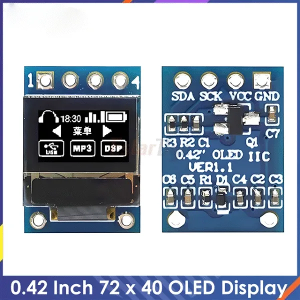 0.42 Inch White OLED Display LCD Module 72X40 Serial Screen White Color I2C IIC/SPI Interface SSD1306 72*40
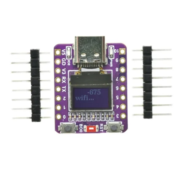 ESP32-C3 OLED Development Board With 0.42 Inch OLED Module Ceramic Antenna Wifi Bluetooth ESP32 Supermini Development Board
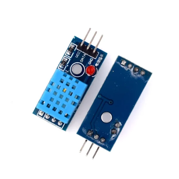 Smart 3pin DHT-11 DHT11 Digital Temperature And Relative Humidity Sensor Module + PCB For Arduino DIY Starter Kit
$1.90
Smart 3pin DHT-11 DHT11 Digital Temperature And Relative Humidity Sensor Module + PCB For Arduino DIY Starter Kit
$1.90
 TRMNL BYOD 7.5" (OG) e-ink DIY Kit, Monochrome e-ink Display 800x480, XIAO ESP32-S3 PLUS,Arduino Compatible,Battery Rechargeable
$115.90
TRMNL BYOD 7.5" (OG) e-ink DIY Kit, Monochrome e-ink Display 800x480, XIAO ESP32-S3 PLUS,Arduino Compatible,Battery Rechargeable
$115.90
Every ESP32 product starts on a dev board. That is the right way to start — you get a working
esp32 pcb certification is one of the few parts of hardware development where the cost of getting it wrong is
An ESP32 iot board design is a system problem wearing a PCB costume. It has to sense something, power itself,
The ESP32-WROOM is probably the most common ESP32 module in the world. It is cheap, well-documented, and appears in thousands
The ESP32-S3 is the part people reach for when their product needs more than the classic ESP32 can give: native
Designing an ESP32 board and assembling it are two different disciplines, and the gap between them is where a lot
No account yet?
Create an Account