ESP32 Dev Board vs Custom PCB: When to Switch
Every ESP32 product starts on a dev board. That is the right way to start — you get a working

Most people meet us through the store. They buy an ESP32-C3 Supermini board or a camera module, it ships, and that is the end of the story. But there is a second half of esp32s.com that a lot of first-time visitors never see, and it is the part we are quietly proudest of: we design custom ESP32 hardware for product teams.
This article is about that half. If you have a working prototype on a dev board and you are trying to turn it into a product, this is the service that does it — and below is exactly what happens when you hire us, from the first email to the files you take to a manufacturer.
We keep them separate on purpose, because combining them into one vague "design services" page is how people end up paying for work they did not need.
ESP32 PCB Design is for when your circuit is not defined yet. You know what the product has to do — sense something, talk to a cloud, run on a battery, fit a case — but you do not know which module, which power architecture, or which connectors get you there. We work from your product brief through module selection, circuit design, layout, and prototype handoff.
Firmware design and firmware flashing can be included in the same quotation if you need them.
PCB Layout is for when you already have a schematic. You have done the circuit work, and you need someone to turn it into a board that can actually be manufactured — placement, routing, the antenna done properly, and fabrication outputs you can hand to a fab without embarrassment. This is the faster, cheaper path, and it is the right one if your schematic is genuinely finished.
If you are not sure which you need, the honest test is this: open your schematic. If it exists and you would bet money on it, you need layout. If it does not exist, or you would not, you need the design service.
We are not a general-purpose layout shop that happens to accept ESP32 work. We do ESP32, and that focus shows up in specific, unglamorous ways.
The antenna is treated as the first constraint, not an afterthought. On a custom ESP32 board, the module's antenna needs a keep-out region with no copper, on any layer, and no components — and it needs the module placed at the board edge with the antenna facing outward. We have written about this at length because it is the single most common reason a custom ESP32 board has terrible Wi-Fi range: someone poured ground under the antenna.
On our layouts, the keep-out is a design rule, not a note someone might remember.
Power is planned around the transmit burst. An ESP32 pulls a short, large current spike when the radio transmits. Regulators sized on average current — which is a very common mistake — brown out exactly when the product is doing its most visible work. We size the supply for the peak and check the decoupling against the reference design.
Programming and debug access is designed in. A board with no way to flash it or probe it is a board you debug by soldering wires to pads. We bring out the programming and test access as a matter of course, because we have all regretted the alternative.
Firmware and hardware are planned together. We offer ESP32 firmware design and flashing as part of a project, which means the board is laid out knowing which pins the firmware needs, which rails it will switch, and where the debug interface lives. When hardware and firmware are designed in the same room, you skip a whole category of integration pain.
If you have used a generalist shop before and spent a week explaining why the antenna cannot be moved, you will recognise the difference immediately.
We do not start work until the scope is agreed, because a design project that starts without a defined finish line is a project that ends in an argument.
Step one: you share your requirements. Send your project brief and whatever files you have. For PCB Design, that is a description of what the product must do, how it is powered, how it connects, the enclosure size, and any reference hardware. For PCB Layout, that is your schematic and netlist, plus the board dimensions, mounting holes, enclosure drawings, and fixed connector positions.
You can also tell us your target quantities, budget, and schedule — those shape the design.
Step two: we confirm the scope. Before any design work starts, we agree the deliverables, the price, the schedule, and the revision process. For PCB Design, the deliverables typically include the schematic and PCB source files in your agreed CAD format, a component list, fabrication and assembly files, design notes, and any agreed firmware source or binaries.
For PCB Layout, they include the layout source files, Gerber and drill files, assembly drawings and placement data, plus design review notes.
Step three: we review and release. We design, we review the design with you, and we prepare the agreed files for your next step — a prototype run, a production order, or a certification submission. Items that need your confirmation are recorded rather than decided silently.
That is the whole loop. Notice that step two exists before step three, and that the deliverables are written down. That is what separates a service engagement from a favour between friends.
The more you send, the better the quote and the shorter the path to work starting.
For PCB Design:
For PCB Layout:
You do not need a perfect package to start the conversation. You need enough for us to tell you honestly whether you are two weeks or two months away from a finished board.
We are a good fit for a few specific kinds of team:
IoT product startups who have a working prototype on a dev board and a rough idea of the case, and who need a first custom board without hiring a hardware team. This is the most common shape of project we take on.
Hardware teams who need layout capacity. Your engineers have done the circuit, but the layout queue is three months deep and the product cannot wait. We take the schematic and return a board.
Overseas teams without a China presence. If your product is going to be manufactured in Shenzhen and you cannot be there, the fact that our designers and factories are in the same city matters. We can coordinate the design with the manufacturing reality rather than handing you an idealised board that no fab will quote.
One of the practical advantages of working with us is that design and manufacturing are not strangers. When your design is ready, the fabrication and assembly path runs through our own ordering line at DIYIPCB, and we support small to medium batch production from 5 to 10,000 units.
That means the board is designed by people who know what the factory will do with it. Panelization, impedance control, the surface finish needed near fine-pitch parts — these are not abstract requirements to us; they are the things we would be checking anyway when the board goes to build.
"Will you sign an NDA?" Yes. We protect projects with NDAs, and we ask that you agree a file-sharing method with us before sending confidential design files. IP ownership of your design remains yours.
"What if I need changes after the first review?" The revision process is agreed with the scope, in step two. You know how revisions work before the work starts, not after you are unhappy.
"Can you do firmware too?" Yes, as part of a project or as a separately quoted service. Firmware source, binaries, flashing instructions, and verification records are agreed deliverables when firmware is in scope.
"Do you only do ESP32?" ESP32 is our specialty — including the S3, C3, and H2 families — but the design and layout discipline applies to the surrounding circuitry and sensors too. The ESP32 focus is why we are good at it, not a limitation on what the board can contain.
You do not need a finished brief to talk to us. Send what you have to [email protected], or reach us through esp32s.com/contactus, and we will tell you which service fits and what it would take.
Design work is a commitment on both sides. We would rather spend twenty minutes up front making sure it is the right project for both of us than discover it three weeks in.
Abstract talk about "design services" is easy to write and hard to trust. So here is what a real engagement looks like, drawn from the shape of projects we take on every week.
Imagine a small team in Europe building a battery-powered environmental sensor. On the bench, it runs on an ESP32-C3 Supermini — one of the cheapest ways to prove an idea works. The firmware reads a temperature and humidity sensor over I2C, wakes every fifteen minutes, and posts a reading to their cloud. It works.
Then reality arrives: the case they want is 42 mm across, the dev board does not fit, battery life is measured in days instead of months, and their first customer wants a hundred units.
That is the moment the ESP32 PCB Design service is for. Over the first conversation, the open questions get pinned down: which C3 variant has the flash they need, whether a module with an integrated antenna can meet their range requirement inside a plastic case, and what the battery actually has to supply given the transmit burst. None of these is a layout question yet. They are product-definition questions, and they decide what the board will be.
The design then moves through circuit definition, module selection, and layout. The antenna keep-out becomes a design rule so it survives every reroute. The power architecture is built around the sleep current, because for this product sleep current is the whole ballgame — a tenth of a milliamp left on overnight turns a promised year of battery life into a marketing problem.
The programming and debug access is brought out so the factory can flash the units and the team can still investigate a field failure.
By the time the design is released, the deliverables are the ones agreed in the scope: the schematic and layout source files, a component list, fabrication and assembly files, and the design notes. If firmware was in scope, the source and binaries and flashing instructions come with it. If it was not, the handoff still anticipates it — the pin map is documented, the debug interface exists, the rails that firmware will switch are the rails the layout routed.
Then the board goes to build through DIYIPCB, and because the people who designed it work in the same city as the factory, the manufacturing conversation is not a translation exercise.
That is the service, end to end. If your project looks like that sensor, you are who we built it for.
We get asked whether being ESP32-specialist is a limitation. It is the opposite, for one practical reason: the expensive mistakes on an ESP32 board are ESP32-specific.
The antenna keep-out is different for a module with a printed antenna than for a chip-down design. The transmit burst has a particular current profile that catches under-sized regulators. The strapping pins have to be at the right levels at reset or the chip boots into the wrong mode. The crystal and its load capacitors follow a reference design that is easy to get subtly wrong.
These are not general layout skills; they are ESP32 knowledge, and knowing them is why our boards work on the first spin more often than a generalist's.
A general layout engineer can route anything. We route ESP32 boards, and we have been doing it since December 2016.
A board that needs a revision is not a failure; it is ordinary engineering, and any honest design house will say so. What matters is how the revision is handled.
Because the revision process is agreed in the scope before work begins, you know going in how changes are treated: what counts as a revision, how it is charged, and how quickly it turns around. If a board comes back and something needs fixing, the path forward is already defined rather than a negotiation under pressure.
We would rather set that expectation honestly than promise a flawless first spin. The first spin usually works; when it does not, the scope we agreed is what keeps the project moving instead of stalling.
Plenty of people get in touch when a conversation is really all they need. That is fine, and it costs nothing.
Send us the state of your project — a dev board on a bench, a half-finished schematic, or a case that does not fit — and ask us which service, if either, applies. We will tell you honestly if layout is not worth doing yet, or if the schematic should be reworked before anyone lays it out. A twenty-minute exchange that saves you a wasted engagement is worth more to us than a job booked too early.
esp32s.com is not only a store. We run two custom hardware services: ESP32 PCB Design for teams whose circuit is not defined yet, and PCB Layout for teams who have a schematic and need a manufacturable board. Both start with a written scope and agreed deliverables, both treat the ESP32 antenna and power as first-class constraints, and both connect cleanly to manufacturing through DIYIPCB.
If you have a prototype on a dev board and a product in mind, this is the part of esp32s.com you were looking for.
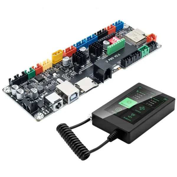 For CNC Engraving Machine Makerbase MKS LS ESP32 PRO GRBL Controller Module Support WIFI Bluetooth Touch Screen Upgrade DLC32
$18.90 – $42.90Price range: $18.90 through $42.90
For CNC Engraving Machine Makerbase MKS LS ESP32 PRO GRBL Controller Module Support WIFI Bluetooth Touch Screen Upgrade DLC32
$18.90 – $42.90Price range: $18.90 through $42.90
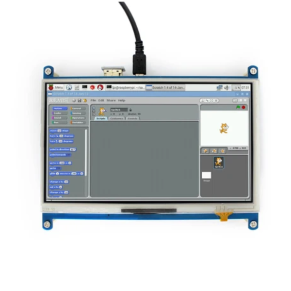 7inch Resistive Touch Screen LCD for for Raspberry Pi 4B/3B+/3A+/3B/2B/B+/A+, 1024x600, HDMI, SPI Touch
$53.90
7inch Resistive Touch Screen LCD for for Raspberry Pi 4B/3B+/3A+/3B/2B/B+/A+, 1024x600, HDMI, SPI Touch
$53.90
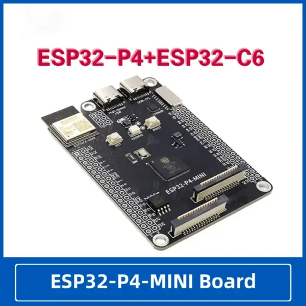 ESP32-P4-MINI Development Board Includes ESP32-C6 mini Support Wifi6 BT Zigbee
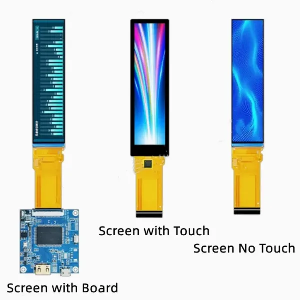 3.71 inch 40PIN TFT LCD IPS Capacitive Screen ST7701S IC SPI+RGB Interface 240*960 HDMI-compatible Interface Drive Board
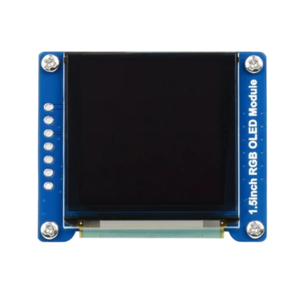 1.5inch RGB OLED display module 128x128, 16-bit high color SPI interface small screen for Raspberry Pi /Arduino/STM32
$22.90
1.5inch RGB OLED display module 128x128, 16-bit high color SPI interface small screen for Raspberry Pi /Arduino/STM32
$22.90
Every ESP32 product starts on a dev board. That is the right way to start — you get a working
Everyone talks about PCB layout, but the schematic is where most of the expensive mistakes actually happen. A layout error
esp32 pcb certification is one of the few parts of hardware development where the cost of getting it wrong is
An ESP32 iot board design is a system problem wearing a PCB costume. It has to sense something, power itself,
The ESP32-WROOM is probably the most common ESP32 module in the world. It is cheap, well-documented, and appears in thousands
The ESP32-S3 is the part people reach for when their product needs more than the classic ESP32 can give: native
No account yet?
Create an Account