Why Solder Wicking is a Reliability Killer
In through-hole technology (THT) assembly, the goal is to create a robust, concave solder fillet that bonds the component lead to the PCB pad and extends slightly up the lead (typically 1.5mm to 2.0mm for Class 2, and more for Class 3).
Solder wicking disrupts this goal. Driven by capillary action, molten solder is drawn upward along the metal component lead, much like water climbing a paper towel. When this happens excessively, the solder is pulled away from the PCB pad. The result is a "starved joint"—a connection that may look acceptable from a top-down visual inspection but lacks the necessary solder volume to provide mechanical strength or reliable electrical conductivity.
For hardware developers and supply chain managers, solder wicking is not just a cosmetic flaw; it is a direct pathway to costly field returns, warranty claims, and expensive manual rework. Understanding the physics behind wicking and implementing strict DFM controls is mandatory for scaling from prototype to high-volume production.
The Physics of Wicking: Understanding the Root Causes
To prevent solder wicking, we must first understand the three primary forces that drive it during the soldering process:
- Capillary Action: The narrow space between the component lead and the wall of the plated through-hole (PTH) acts as a capillary tube. If the gap is too large, or if the lead is too long, molten solder is naturally drawn upward by surface tension.
- Thermal Imbalance (The "Heat Sink" Effect): Component leads (especially thick ones or those connected to internal ground planes) act as heat sinks. If the PCB and component are not adequately preheated, the cold lead rapidly absorbs heat from the molten solder wave. This causes the solder to solidify prematurely as it climbs the lead, freezing the wicking effect in place and preventing the solder from flowing back down to the pad.
- Flux Activity Depletion: Flux is designed to remove oxides and lower the surface tension of molten solder, promoting wetting on the pad. If the flux is depleted before the board hits the solder wave (due to excessive preheat or long conveyor times), the solder will seek the path of least resistance, which is often up the cleaner, hotter component lead.
Top 3 Solder Wicking Pain Points in Manufacturing (And How We Solve Them)
As a hardware developer, your goal is a high first-pass yield. Here are the most common wicking-related failures and how a professional manufacturing partner mitigates them:
1. The "Starved Joint" and Mechanical Failure
The Pain Point: The solder fillet on the top side of the board is concave or completely missing, while a large, bulbous mass of solder is visible on the bottom or hidden up the lead. In applications subject to thermal cycling or vibration, this joint will crack, leading to intermittent connectivity.
Our Solution: We enforce strict lead length and hole-size DFM rules. By optimizing the ratio between the component lead diameter and the finished hole size, we minimize the capillary gap. Furthermore, our assembly team uses precise lead-clinching or forming techniques to physically anchor the component to the pad, acting as a mechanical barrier to upward solder flow.
2. Inconsistent Preheating Leading to Thermal Shock
The Pain Point: Boards with mixed technology (e.g., heavy connectors alongside small resistors) experience uneven heating. Heavy leads remain cold, aggressively wicking solder, while smaller components overheat.
Our Solution: We utilize advanced, multi-zone thermal profiling for our wave and selective soldering machines. We map the exact temperature gradient across the entire PCB, adjusting preheat zones (typically targeting 100°C to 130°C at the top side of the board) to ensure all components reach thermal equilibrium before contacting the solder wave. This eliminates the heat-sink effect that drives wicking.
3. Flux Depletion and Oxidation
The Pain Point: Long preheat times or improper flux application cause the flux to burn off before soldering. The solder fails to wet the pad properly and instead wicks up the lead, creating dull, grainy, and unreliable joints.
Our Solution: We employ automated, uniform flux spraying systems (foam or micro-drop) calibrated to the specific solder paste and board density. We also strictly monitor conveyor speeds and preheat times to ensure the flux remains active and volatile carriers are properly evaporated without degrading the rosin or no-clean activators.
The Ultimate DFM Checklist to Prevent Solder Wicking
Preventing wicking starts in the CAD design phase. To ensure your design is 100% manufacturable, your layout must adhere to these industry-proven DFM rules, aligned with IPC-A-610 (Acceptability of Electronic Assemblies) standards:
- Optimize Hole-to-Lead Ratio: The finished plated hole diameter should be only 0.2mm to 0.3mm (8 to 12 mils) larger than the component lead diameter. Example: For a 0.6mm lead, the finished hole should be 0.8mm to 0.9mm. Oversized holes are the #1 cause of capillary wicking.
- Control Lead Protrusion Length: The component lead extending above the top solder mask should be strictly controlled. For standard wave soldering, a protrusion of 1.5mm to 2.0mm is ideal. If leads are too long (>2.5mm), they will act as a wick. If they are flush or cut too short, inspection is impossible, and joint strength is compromised.
- Thermal Relief Design: For through-hole pins connected to large copper pours or ground planes, use thermal relief spokes (typically 4 spokes). This slows down heat dissipation into the plane, preventing the pin from acting as a massive heat sink that triggers wicking.
- Solder Mask Dams: Ensure a continuous solder mask dam between adjacent through-hole pads. This prevents solder from wicking laterally across the board surface and encourages it to stay confined to the intended fillet area.
- Component Selection: For high-reliability applications, specify components with "kinked" or "formed" leads rather than straight leads. The kink provides a physical anchor against the PCB surface, resisting upward capillary pull.
Why Partner with a Professional Turnkey PCBA Manufacturer?
Solder wicking is a complex defect that sits at the intersection of bare-board fabrication (hole sizing, copper weight) and assembly processing (thermal profiling, fluxing). Sourcing the bare board from one vendor and the assembly from another often leads to finger-pointing when wicking defects occur.
You need a unified, accountable partner who controls the entire process. We bridge the gap between theoretical design and high-yield manufacturing reality:
- Proactive DFM & Stack-up Engineering: Before production begins, our engineering team reviews your CAD files. We automatically flag oversized holes, missing thermal reliefs, or excessive lead lengths, providing you with a detailed, free DFM report to eliminate wicking risks before any metal is cut.
- Seamless Prototyping to Turnkey Assembly: Whether you are building a complex industrial control board or a high-power LED driver, our turnkey PCB assembly manufacturing service handles the entire lifecycle. We manage the BOM, source authentic components, and utilize precision wave/selective soldering with real-time thermal profiling to guarantee perfect, IPC-compliant solder fillets every time. Discover how we simplify your workflow: PCB Prototype & Turnkey PCB Assembly Manufacturing.
- Scalable OEM/ODM Bulk Production: When your design is validated, scaling to mass production requires unwavering consistency. We utilize 3D Automated Optical Inspection (AOI) and X-ray systems specifically calibrated to measure solder fillet height and volume, ensuring every single unit meets strict IPC-A-610 Class 2 or Class 3 standards. Request a detailed, competitive quote for your next large-scale project: OEM/ODM Bulk Inquiry.
Frequently Asked Questions (FAQ)
Q1: Can solder wicking be fixed after it happens?
A: While manual rework (using a soldering iron and solder wick/braid to remove excess solder, followed by re-tinning) is possible, it is highly discouraged for high-reliability products. Rework introduces thermal stress, risks pad lifting, and is cost-prohibitive in bulk production. Prevention via DFM and process control is always the superior strategy.
Q2: Does solder wicking only happen in wave soldering?
A: No. While it is most common in wave and selective soldering due to the large volume of molten solder, wicking can also occur during manual hand-soldering if the operator applies the iron to the lead for too long before touching the pad, or if excessive solder is applied.
Q3: What is the difference between solder wicking and solder bridging?
A: Solder wicking is the vertical movement of solder up a component lead, resulting in a starved pad. Solder bridging is the horizontal, unintended flow of solder between two adjacent pins or pads, creating a short circuit. Both are wave soldering defects but require different DFM and process solutions.
Q4: How do you verify that solder fillets meet IPC standards?
A: We employ a multi-tiered inspection process. This includes top-and-bottom 3D Automated Optical Inspection (AOI) to measure fillet geometry, and for critical, high-density, or double-sided THT boards, we utilize 3D X-ray inspection to verify internal hole fill and ensure no voids or wicking defects are hidden from view.
Master the Process, Guarantee the Reliability
Solder wicking is not an unavoidable quirk of electronics manufacturing; it is a predictable physical phenomenon that can be entirely engineered out of your production process. By understanding the capillary and thermal dynamics at play, and by enforcing strict DFM rules for hole sizes and lead lengths, you protect your product from premature field failures.
However, achieving this consistently requires more than just a good design; it requires a manufacturing partner with deep process expertise. Don’t leave your product’s reliability to chance. Partner with a team that controls the entire fabrication and assembly workflow, ensuring every solder joint is robust, reliable, and built to last.

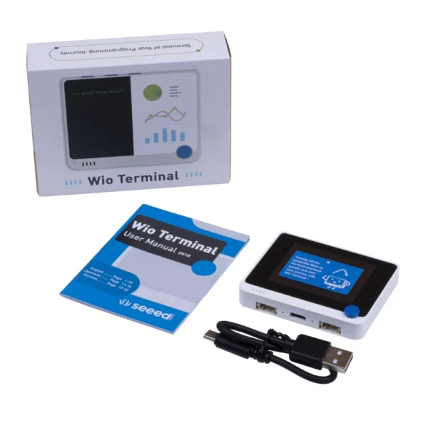 Wio Terminal Microcontroller Dev Board, 2.4” LCD Screen,ATSAMD51 Core,Realtek RTL8720DN, Grove,Raspberry Pi,Arduino,MicroPython
$38.90
Wio Terminal Microcontroller Dev Board, 2.4” LCD Screen,ATSAMD51 Core,Realtek RTL8720DN, Grove,Raspberry Pi,Arduino,MicroPython
$38.90
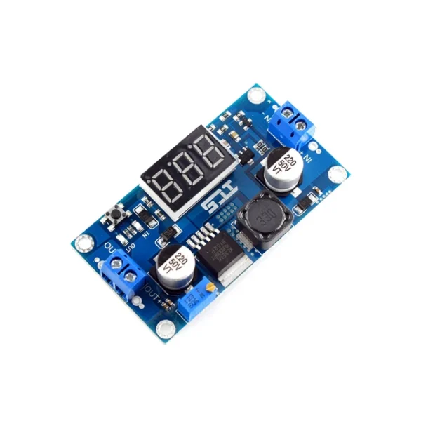 Upgraded Version XL6009 Boost Module DC-DC 5V-32V To 5V-40V 4A Adjustable Step Up Power Supply Module with Digital Display
$3.50
Upgraded Version XL6009 Boost Module DC-DC 5V-32V To 5V-40V 4A Adjustable Step Up Power Supply Module with Digital Display
$3.50
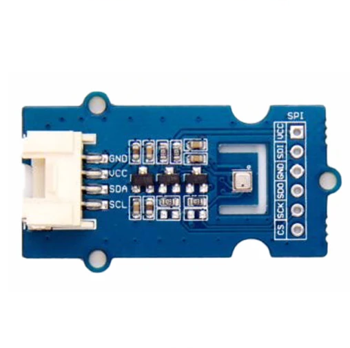 Grove Temperature Humidity Barometer Sensor Breakout Board for Bosch BMP280 High Accuracy Environmental Detection measurement
$16.90
Grove Temperature Humidity Barometer Sensor Breakout Board for Bosch BMP280 High Accuracy Environmental Detection measurement
$16.90
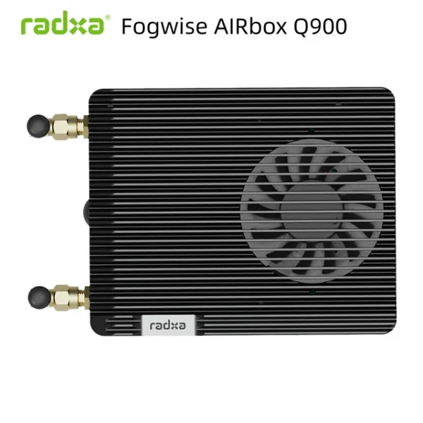 Radxa Fogwise AIRbox Q900, Edge AI, IQ-9075, 200 TOPS@INT8 (Sparse) ,Octa-core CPU high-performance GPU,36GB RAM 128UFS
$895.90
Radxa Fogwise AIRbox Q900, Edge AI, IQ-9075, 200 TOPS@INT8 (Sparse) ,Octa-core CPU high-performance GPU,36GB RAM 128UFS
$895.90
 ESP32-S3 1.54inch LCD N16R8 Development Board Display Screen Wifi Weather Station TimeClock DeepSeek For XiaoZhi AI Chat Box