Why PCB Silkscreen is Critical for Manufacturing Yield
In the hierarchy of PCB layers, the silkscreen is often mistakenly viewed as merely "cosmetic." Hardware designers sometimes treat it as an afterthought, cramming logos, version numbers, and component designators into tight spaces without considering the manufacturing reality.
This is a critical engineering oversight. The silkscreen is the primary communication tool between the CAD design and the physical assembly line. It guides automated optical inspection (AOI) systems, assists pick-and-place machine verification, and is absolutely essential for human technicians during debugging, testing, and field repair.
More importantly, silkscreen ink is a physical material with thickness and thermal properties. If it is placed incorrectly, it directly interferes with the soldering process. Understanding the manufacturing constraints and DFM (Design for Manufacturability) rules of PCB silkscreen is mandatory for any team aiming to achieve high first-pass yield and scalable OEM/ODM bulk production.
PCB Silkscreen Manufacturing Processes: Choosing the Right Method
Not all silkscreens are created equal. The application method significantly impacts resolution, durability, and cost. A professional manufacturer will select the optimal process based on your design's complexity and density.
1. Liquid Photoimageable (LPI) Silkscreen (The Industry Standard)
- How it works: Similar to the solder mask process, a liquid epoxy ink is coated onto the board, exposed to UV light through a film mask, and developed.
- Pros: High resolution, excellent adhesion to the substrate, and a smooth, thin finish. It is the most cost-effective and widely used method for 90% of modern PCBs.
- Best For: Standard consumer electronics, industrial controllers, and boards with moderate component density.
2. Direct Legend Printing (DLP) / Inkjet Printing
- How it works: An automated inkjet printer directly deposits UV-curable ink onto the PCB surface, guided directly by the CAD data (no film masks required).
- Pros: Exceptional resolution (capable of printing very small text and complex QR codes/barcodes), perfectly aligned, and ideal for highly dense HDI boards.
- Best For: High-density interconnect (HDI) boards, medical devices requiring traceability barcodes, and prototypes where rapid turnaround without film tooling is required.
3. Manual Screen Printing (Legacy Method)
- How it works: Ink is physically pushed through a woven mesh screen onto the board.
- Pros: Very low setup cost for simple, large-text designs.
- Cons: Low resolution, prone to misalignment, and thick ink deposits that can cause assembly issues. Rarely used in modern, high-reliability manufacturing.
Top 3 Silkscreen Manufacturing Pain Points (And How We Solve Them)
As a hardware developer or supply chain manager, your goal is to eliminate preventable assembly defects. Here are the most common silkscreen-related failures and how a professional manufacturing partner mitigates them:
1. Solder Joint Defects Caused by Pad Contamination
The Pain Point: If silkscreen ink overlaps or sits too close to a solder pad, it acts as a barrier. During reflow or wave soldering, the solder paste cannot properly wet the copper pad. This results in "dry joints," weak mechanical bonds, or intermittent electrical connections that fail under vibration or thermal cycling.
Our Solution: We enforce strict pad clearance rules during our automated and manual DFM review. Our CAM engineers ensure a minimum keep-out zone between the silkscreen and the exposed pad. If your design violates this, we will proactively adjust the silkscreen layout or contact you for approval before fabrication begins.
2. Illegible Text and AOI Inspection Failures
The Pain Point: Designers often use fonts that are too small (e.g., < 40 mil height) or place light-colored text over dark solder masks (or vice versa) without checking contrast. This makes component identification impossible for assembly technicians and causes Automated Optical Inspection (AOI) systems to throw false errors.
Our Solution: We apply standardized text sizing and contrast guidelines. We recommend a minimum character height of 40-50 mil (1.0 - 1.27mm) and a minimum line width of 6 mil (0.15mm). We also verify that the chosen silkscreen color (typically white, black, or yellow) provides maximum optical contrast against the solder mask color for optimal machine and human readability.
3. Ink Delamination and Discoloration During Reflow
The Pain Point: During lead-free reflow soldering, peak temperatures can reach 260°C. Low-quality silkscreen inks or improper curing can cause the ink to yellow, crack, or delaminate (peel off), especially on surface finishes like ENIG or Immersion Silver.
Our Solution: We utilize high-Tg (Glass Transition Temperature), thermally stable epoxy inks specifically formulated for lead-free assembly profiles. Our curing processes are strictly controlled to ensure maximum cross-linking and adhesion to the specific surface finish of your board, guaranteeing the legend remains intact throughout the product's lifecycle.
The Ultimate DFM Checklist for PCB Silkscreen
To ensure your design is 100% manufacturable and assembly-ready, your CAD layout must adhere to these industry-proven DFM rules, aligned with IPC standards:
- Minimum Line Width and Spacing: Maintain a minimum silkscreen line width and spacing of 6 mil (0.15mm) for LPI processes, and 4 mil (0.10mm) for Direct Legend Printing (DLP).
- Component Pad Clearance: Keep silkscreen at least 4 to 6 mil (0.10 to 0.15mm) away from the edge of any exposed solder pad. Never allow silkscreen to overlap a pad.
- Text Height and Font: Use vector fonts (not rasterized images). The minimum recommended character height is 40 mil (1.0mm) to ensure legibility after manufacturing tolerances are applied.
- Avoid Vias and Test Points: Do not place silkscreen over uncovered vias or bare copper test points, as the ink will prevent proper probing or soldering.
- Standardize Orientation: Orient all component designators (e.g., R1, C5, U3) in the same direction (preferably readable from left to right or bottom to top) to drastically speed up manual assembly and debugging.
Why Partner with a Professional Turnkey PCBA Manufacturer?
The silkscreen layer is the bridge between your digital design and physical reality. Sourcing bare boards from a low-cost vendor who ignores silkscreen DFM, and then sending them to a separate assembly house, is a recipe for finger-pointing when soldering defects occur.
You need a unified, accountable partner who controls the entire process. We bridge the gap between theoretical design and high-yield manufacturing reality:
- Proactive DFM & Silkscreen Optimization: Before production begins, our engineering team reviews your Gerber and assembly files. We automatically flag silkscreen-to-pad violations, illegible text sizes, and contrast issues, providing you with a detailed, free DFM report to eliminate assembly risks before any ink is printed.
- Seamless Prototyping to Turnkey Assembly: Whether you are building a complex medical device requiring precise barcode tracking or a rugged industrial controller, our turnkey PCB assembly manufacturing service handles the entire lifecycle. We manage the BOM, source authentic components, and utilize our optimized silkscreen legends to ensure flawless pick-and-place alignment and AOI verification. Discover how we simplify your workflow: PCB Prototype & Turnkey PCB Assembly Manufacturing.
- Scalable OEM/ODM Bulk Production: When your design is validated, scaling to mass production requires unwavering consistency. We utilize high-precision LPI or DLP silkscreen processes, coupled with strict IPC-A-610 Class 2/3 visual inspection standards, to guarantee every single unit is perfectly marked and reliably assembled. Request a detailed, competitive quote for your next large-scale project: OEM/ODM Bulk Inquiry.
Frequently Asked Questions (FAQ)
Q1: Can silkscreen be placed on both the top and bottom layers of a PCB?
A: Yes. Silkscreen can be applied to both sides of the board. However, placing it on the bottom layer is typically reserved for essential information (like part numbers, revision codes, or polarity markings for bottom-mounted components), as top-side silkscreen is more critical for SMT assembly and debugging.
Q2: What is the best silkscreen color for a green PCB?
A: White is the industry standard and provides the highest contrast against a green solder mask, ensuring maximum legibility for both human technicians and AOI cameras. Black can be used for aesthetic purposes but may reduce contrast. Yellow is sometimes used for high-voltage warning areas.
Q3: Can I print a complex logo or QR code using silkscreen?
A: Yes, but the method matters. For complex logos or scannable QR codes, we highly recommend Direct Legend Printing (DLP). DLP offers the high resolution required to maintain the sharp edges of a QR code, ensuring it remains scannable after the manufacturing process, whereas traditional LPI or manual screening may blur fine details.
Q4: Does silkscreen affect the impedance of high-speed traces?
A: Generally, no. Silkscreen ink is a non-conductive dielectric material. However, if thick silkscreen is placed directly over a high-frequency RF trace, it can slightly alter the local dielectric constant, potentially causing minor impedance variations. Best practice dictates keeping silkscreen away from critical high-speed or RF transmission lines.
Precision Silkscreen is the Mark of Professional Manufacturing
PCB silkscreen is far more than a cosmetic afterthought; it is a critical functional layer that dictates assembly efficiency, inspection accuracy, and long-term maintainability. Ignoring silkscreen DFM rules is a direct invitation to soldering defects, rework delays, and field failures.
By adhering to strict design guidelines and partnering with a manufacturer that treats silkscreen engineering with the same rigor as copper routing, you transform a potential manufacturing bottleneck into a seamless, scalable advantage.

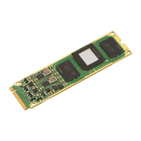 Radxa AICore AX-M1, AI Acceleration Module, Axera AX8850, 24 TOPS@INT8, 8GB RAM
$349.80
Radxa AICore AX-M1, AI Acceleration Module, Axera AX8850, 24 TOPS@INT8, 8GB RAM
$349.80
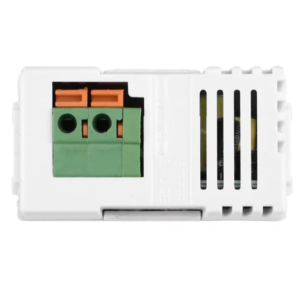 Type 128 USB Power Module 220V Socket 5V 2.1A 1A Mobile Phone Charger Module Switch Adapter Transformer Socket Electronic Kit
$3.90 – $5.90Price range: $3.90 through $5.90
Type 128 USB Power Module 220V Socket 5V 2.1A 1A Mobile Phone Charger Module Switch Adapter Transformer Socket Electronic Kit
$3.90 – $5.90Price range: $3.90 through $5.90
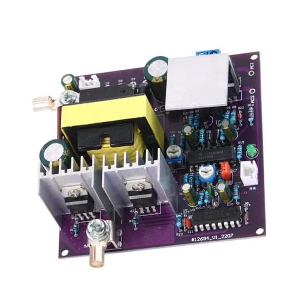 300W Corrected Sine Wave Output 50Hz Inverter 12V To 220V Inverter Power Supply Energy Storage DC-AC Boost Circuit Board
$10.90
300W Corrected Sine Wave Output 50Hz Inverter 12V To 220V Inverter Power Supply Energy Storage DC-AC Boost Circuit Board
$10.90
 10pin Alligator Clip to Breadboard Jumper Wire Dupont Cable 20cm Male Female Test Lead for Arduino Microbit Nano LED Strip
$2.90 – $4.80Price range: $2.90 through $4.80
10pin Alligator Clip to Breadboard Jumper Wire Dupont Cable 20cm Male Female Test Lead for Arduino Microbit Nano LED Strip
$2.90 – $4.80Price range: $2.90 through $4.80
 FM Radio DIY Electronics Kit Bluetooth 5.0-Compatible Speaker with Voice-activated Level Indicator DIY Electronics Kit
$10.90
FM Radio DIY Electronics Kit Bluetooth 5.0-Compatible Speaker with Voice-activated Level Indicator DIY Electronics Kit
$10.90