The High Stakes of IoT Hardware Prototyping
As an IoT hardware developer or startup founder in 2026, you know the drill: you’ve spent weeks perfecting your schematic in KiCad or Altium Designer. You’ve chosen the perfect ESP32-S3 for its edge AI capabilities, or the ESP32-C6 for its native Wi-Fi 6 and Matter support. You send off your Gerber files, wait two weeks, and the boards arrive. You populate the first unit, apply power, and… nothing. Or worse, the Wi-Fi range is a fraction of what the datasheet promises.
A failed PCB spin doesn’t just cost money; it costs invaluable time, delays investor demos, and drains team morale.
The harsh reality is that generic PCB design rules are not enough for advanced RF SoCs like the ESP32 family. To ensure your first prototype works flawlessly, your design must adhere to strict Design for Manufacturing (DFM) and Design for Assembly (DFA) guidelines.
At esp32s.com, we have assembled tens of thousands of custom ESP32-based boards for clients worldwide. Through this experience, we’ve identified the most common, costly mistakes developers make—and exactly how a specialized turnkey PCB assembly service can eliminate these risks before you even hit "order."
Why ESP32-S3 and ESP32-C6 Require Specialized DFM Attention
The ESP32 family is incredibly powerful, but that power comes with physical constraints. The ESP32-S3 integrates a 2.4 GHz Wi-Fi and Bluetooth 5 (LE) radio with vector instructions for AI acceleration. The ESP32-C6 adds 802.11ax (Wi-Fi 6) capabilities.
These high-frequency radios are highly sensitive to their physical environment on the PCB. A generic 2-layer board layout that works perfectly for a simple Arduino Uno will almost certainly fail when applied to an ESP32 RF circuit. Issues like impedance mismatch, poor grounding, and inadequate thermal relief can turn a brilliant software concept into an unusable piece of silicon.
Furthermore, from a manufacturing perspective, the trend toward miniaturization means more 0402 or even 0201 passive components, and denser BGA or QFN packages (like the ESP32-WROOM or WROVER modules). This requires precise solder paste stencils and advanced Pick-and-Place accuracy that hobbyist methods cannot achieve.
Top 4 Critical DFM Mistakes in ESP32 Prototyping (And How to Fix Them)
1. RF Antenna Keep-Out Zone Violations
The Pain Point: The most common complaint we hear is, "My ESP32 board works, but the Wi-Fi/Bluetooth range is only 2 meters." The Technical Reality: The PCB trace antenna (or the area surrounding a chip antenna) requires a strict "keep-out zone." For ESP32 modules, this means no copper pours (neither ground nor signal), no vias, and no components on any layer directly beneath or adjacent to the antenna feed line and radiating element. The DFM Fix:
- Maintain a minimum clearance of 2mm to 3mm around the antenna area on all layers.
- Ensure the feed line has a controlled impedance of 50 ohms. If you are using a 2-layer board, this often requires a specific trace width (e.g., ~1.2mm on FR-4 with 1.6mm thickness), which must be verified with your manufacturer’s impedance calculator.
- Do not route high-speed digital signals (like SPI or high-frequency PWM) near the RF section to prevent harmonic interference.
2. Improper Decoupling Capacitor Placement
The Pain Point: The ESP32 randomly reboots under load, especially when the Wi-Fi radio transmits at peak power (which can draw instantaneous current spikes up to 500mA+). The Technical Reality: Decoupling capacitors are meant to act as local energy reservoirs. If they are placed too far from the ESP32’s VDD pins, the parasitic inductance of the trace negates their effectiveness. The DFM Fix:
- Place the critical 100nF (0.1µF) decoupling capacitors as close to the ESP32 VDD/VDD3P3 pins as physically possible (ideally < 5mm).
- Use 0402 or 0603 package sizes for these capacitors to minimize pad inductance.
- Crucial DFA Tip: Route the trace from the ESP32 pin to the capacitor pad first, and then from the capacitor to the via going to the power plane. Do not place the via between the pin and the capacitor.
3. USB Differential Pair Impedance Mismatch
The Pain Point: The ESP32-S3 features native USB OTG. Many developers find that their board is not recognized by a PC, or the connection is highly unstable. The Technical Reality: USB 2.0 requires a strict 90-ohm differential impedance for the D+ and D- lines. The DFM Fix:
- Route the D+ and D- traces together, maintaining consistent spacing.
- Ensure length matching between the two traces. The mismatch should be less than 5mm (ideally < 2mm) to prevent signal skew.
- Avoid routing these pairs near switching power supplies (DC-DC converters) or crystal oscillators to prevent EMI (Electromagnetic Interference).
4. BOM Obsolescence and Module Substitution Blind Spots
The Pain Point: Your design is perfect, but the specific ESP32 variant you specified (e.g., ESP32-WROOM-32E) has a 40-week lead time, or the price has tripled, halting your prototype build. The Technical Reality: The semiconductor supply chain remains dynamic. Relying on a single, highly specific part number without a validated alternative is a major project risk. The DFM Fix:
- Design your footprint to be compatible with multiple variants if possible (e.g., ensuring the pinout matches both WROOM and WROVER series, noting that WROVER requires additional PSRAM routing).
- Partner with a PCBA provider that has real-time supply chain visibility and the engineering expertise to suggest form-fit-function validated alternatives without requiring a full PCB respin.
Understanding DFM rules is only half the battle. Executing them requires the right manufacturing partner. Many developers attempt to source bare PCBs from one vendor, buy components from Digi-Key or Mouser, and assemble the boards locally or via a disjointed assembly house. This "fragmented" approach introduces massive friction:
- Component Sourcing Delays: You spend days tracking down 10 missing passive components.
- Assembly Miscommunication: The assembly house doesn’t understand the RF sensitivity of your board and uses the wrong solder paste profile, causing cold joints on the ESP32 module.
- Hidden Costs: Shipping components between three different locations eats up your budget and timeline.
When you choose a dedicated turnkey partner like esp32s.com, we handle the entire lifecycle under one roof:
- Intelligent DFM/DFA Review: Before any money is spent, our engineering team reviews your Gerber and BOM files. We proactively flag issues like the antenna keep-out violations or capacitor placements mentioned above.
- End-to-End Component Sourcing: We leverage our established supply chain networks to procure all components, including hard-to-find ICs, often at better rates than retail distributors. We also handle legitimate cross-referencing if your primary choice is out of stock.
- Advanced Manufacturing: We utilize high-precision SMT lines capable of handling 0201 components and fine-pitch QFN/BGA packages, followed by rigorous AOI (Automated Optical Inspection) and optional X-Ray inspection for hidden solder joints.
- Functional Testing: We can work with you to develop basic power-on or functional test fixtures, ensuring the board works before it ships to your desk.
The result? You reduce your time-to-market by 30% to 50%, eliminate the administrative burden of supply chain management, and receive a fully tested, ready-to-flash ESP32 board.
Your Pre-Flight Checklist Before Uploading Gerber Files
To ensure your next ESP32 prototype is a success, run through this quick checklist before submitting your files for manufacturing:
- RF Clearance: Verified at least 2-3mm keep-out zone under and around the ESP32 antenna.
- Impedance Control: Specified 50-ohm single-ended (RF) and 90-ohm differential (USB) impedance requirements in your fabrication notes.
- Decoupling: Confirmed 100nF capacitors are placed within 5mm of all ESP32 VDD pins, with correct via routing.
- BOM Validation: Checked that all part numbers in your BOM include manufacturer part numbers (MPN), not just generic descriptions.
- Centroid File: Generated a complete Pick-and-Place (Centroid) file with accurate X/Y coordinates and rotation angles.
- Assembly Drawing: Included a PDF assembly drawing highlighting any special instructions (e.g., "Do not place solder mask on RF trace," or "Keep this area component-free").
Ready to Build Your ESP32 Prototype Right the First Time?
Don’t let preventable DFM mistakes or supply chain headaches delay your IoT innovation. Your hardware deserves a manufacturing partner that understands the unique intricacies of the ESP32 ecosystem.
Here is our promise to you:
- Free Professional DFM Check: Upload your files, and our engineers will review them for manufacturability at no cost.
- Transparent, Upfront Pricing: No hidden fees. You’ll know your total cost before production begins.
- Rapid Turnaround: Get your fully assembled, tested boards in your hands faster than you thought possible.
Stop guessing and start building.
Frequently Asked Questions (FAQ)
Q: What is the minimum order quantity (MOQ) for turnkey PCB assembly at esp32s.com?
A: We cater specifically to prototyping and low-to-medium volume production. Our MOQ starts as low as 5 to 10 pieces, making us the ideal partner for hardware startups and iterative development phases.
Q: Can you help if my specified ESP32 module is out of stock?
A: Absolutely. Our procurement team has deep expertise in the ESP32 product line. If your specified part has a long lead time, we will proactively suggest validated, pin-compatible alternatives (e.g., switching between certain WROOM variants) and get your approval before proceeding.
Q: What file formats do you need for a turnkey quote?
A: To provide an accurate and fast quote, we require:
- Gerber files (RS-274X format preferred).
- A complete BOM (Bill of Materials) in Excel or CSV format, including Manufacturer Part Numbers (MPNs).
- A Centroid (Pick-and-Place) file for SMT assembly.
Q: Do you offer testing for assembled ESP32 boards?
A: Yes. All boards undergo standard AOI (Automated Optical Inspection). For additional assurance, we can implement custom Functional Circuit Testing (FCT) or power-on testing based on your specific requirements. Please mention this in your order notes.

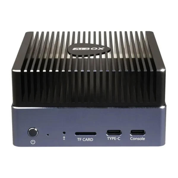 FIREFLY AIBOX-3588 Rockchip RK3588 for IoT Automation Machine Vision 5G AI Edge Computer Embedded PC
$310.80 – $685.90Price range: $310.80 through $685.90
FIREFLY AIBOX-3588 Rockchip RK3588 for IoT Automation Machine Vision 5G AI Edge Computer Embedded PC
$310.80 – $685.90Price range: $310.80 through $685.90
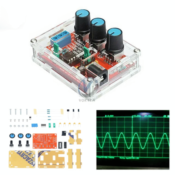 XR2206 High Precision Signal Generator DIY Kit Sine Triangle Square Waves 1Hz 1MHz Frequency Range Adjustable Frequency
$5.90
XR2206 High Precision Signal Generator DIY Kit Sine Triangle Square Waves 1Hz 1MHz Frequency Range Adjustable Frequency
$5.90
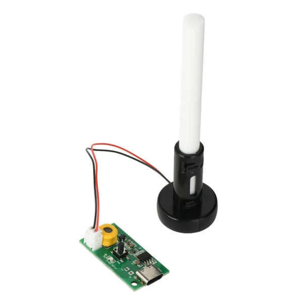 USB Mini Humidifier DIY Kits Mist Maker and Driver Circuit Board Ultrasonic Atomization Control Board Type C Interface
$2.90 – $3.90Price range: $2.90 through $3.90
USB Mini Humidifier DIY Kits Mist Maker and Driver Circuit Board Ultrasonic Atomization Control Board Type C Interface
$2.90 – $3.90Price range: $2.90 through $3.90
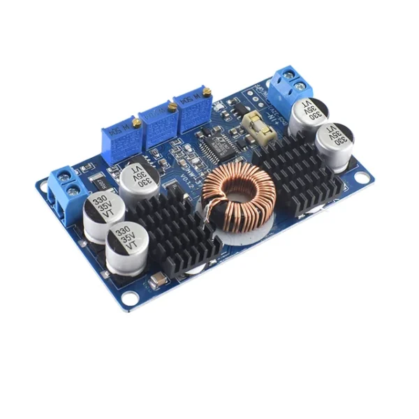 LTC3780EG LTC3780 DC-DC 5-32V to 1V-30V 10A Automatic Step Up Down Regulator Charging Module Power Supply Boost
$10.90
LTC3780EG LTC3780 DC-DC 5-32V to 1V-30V 10A Automatic Step Up Down Regulator Charging Module Power Supply Boost
$10.90
 3.3V 16*2 Character LCD Display LCM 1602 16X2 162 Screen HD44780 Yellow/Blue/Gray Color For 51 STM32 R3