Why PTH Integrity Dictates PCB Reliability
In modern electronics, the Plated Through Hole (PTH) is often taken for granted. Designers place a via or a component footprint, and the CAD software assumes the connection will work. However, from a manufacturing and reliability standpoint, the PTH is the most vulnerable point in a multilayer printed circuit board.
A PTH must survive the mechanical stress of drilling, the chemical aggression of desmearing and plating, and the extreme thermal shock of multiple lead-free reflow soldering cycles (peaking at ~260°C). If the copper plating inside the hole is too thin, discontinuous, or subjected to excessive thermal expansion, the connection will fail.
Understanding the physics and manufacturing constraints of PTHs is not optional; it is a mandatory discipline for any hardware team aiming to achieve high first-pass yields and long-term product reliability.
The Anatomy of a Plated Through Hole: A Manufacturing Perspective
To design for manufacturability, you must understand what happens inside the hole. A standard PTH consists of several critical elements:
- The Drill Hole: The physical void created by a CNC router or laser. Its accuracy dictates the final alignment of the hole.
- The Copper Barrel: The electroplated copper lining the inside of the hole. Per IPC-6012 Class 2/3 standards, this barrel must typically be a minimum of 20µm (0.8 mil) to 25µm (1 mil) thick to ensure adequate current carrying capacity and mechanical strength.
- The Annular Ring: The donut-shaped copper pad surrounding the hole on the outer layers. A sufficient annular ring is critical to prevent "breakout" (where the drill hits the edge of the pad), which compromises the connection.
- The Solder Fillet: For component-mounting PTHs, the molten solder that flows up the barrel and onto the pad, creating the final mechanical and electrical bond.
Top 4 PTH Manufacturing Pain Points (And How We Solve Them)
As a hardware developer or supply chain manager, your goal is to eliminate preventable field failures. Here are the most common PTH-related defects and how a professional manufacturing partner mitigates them:
1. Barrel Cracking (The "Z-Axis" Threat)
The Pain Point: FR-4 substrates expand significantly along the Z-axis (thickness) when heated. If the Z-axis CTE of the substrate is much higher than that of the copper barrel, the substrate expands faster than the copper during reflow soldering. This exerts immense tensile stress on the copper barrel, eventually causing it to crack, especially in the middle of the board thickness.
Our Solution: We proactively recommend High-Tg (Glass Transition Temperature) and Low-CTE materials (e.g., Tg ≥ 170°C) for boards undergoing multiple reflow cycles or operating in high-temperature environments. Additionally, we strictly control our plating chemistry to ensure uniform, ductile copper deposition that can withstand thermal stress.
2. Plating Voids and Nodules
The Pain Point: A "void" is a spot inside the hole where no copper was deposited. This creates an open circuit or a high-resistance connection that may work initially but fail under vibration or thermal cycling. Voids are often caused by trapped air bubbles, poor hole wall preparation (resin smear), or contaminated plating baths.
Our Solution: Our manufacturing process includes a rigorous plasma or chemical desmear process to clean the hole walls and provide a micro-rough surface for copper adhesion. We utilize advanced pulse-plating technology and continuous bath filtration to ensure 100% throw-power (the ability to plate evenly deep inside the hole), eliminating voids.
3. Exceeding the Aspect Ratio Limit
The Pain Point: The "Aspect Ratio" is the ratio of the PCB thickness to the finished hole diameter (e.g., a 1.6mm thick board with a 0.2mm hole has an 8:1 aspect ratio). If the hole is too small relative to the board thickness, plating solutions cannot penetrate to the center, resulting in a "dog-bone" effect (thick copper at the ends, thin or no copper in the middle). Our Solution: Our CAM (Computer-Aided Manufacturing) engineers automatically calculate the aspect ratio of every design. If a design exceeds our standard capability (typically 8:1 for standard through-holes, or up to 10:1 for advanced HDI), we will proactively flag it and recommend increasing the hole diameter or utilizing blind/buried microvias instead.
4. Solder Wicking in Through-Hole Components
The Pain Point: During wave soldering, capillary action can draw molten solder too far up the component lead and into the PTH, leaving a "starved" joint on the top side of the board. This is often exacerbated by an oversized hole-to-lead ratio.
Our Solution: We enforce strict DFM rules for hole sizing. The finished hole diameter should only be 0.2mm to 0.3mm larger than the component lead. We also optimize the wave soldering thermal profile and flux application to ensure proper wetting without excessive wicking.
The Ultimate DFM Checklist for Plated Through Holes
To ensure your design is 100% manufacturable, your CAD layout must adhere to these industry-proven DFM rules, aligned with IPC standards:
- Minimum Annular Ring: Maintain a minimum annular ring of 4 mil (0.1mm) for standard fabrication, and 5 mil (0.127mm) for Class 3 (high-reliability) applications to prevent drill breakout.
- Hole-to-Copper Clearance: Keep a minimum clearance of 8 mil (0.2mm) between the edge of the finished hole and any adjacent copper traces or polygons to prevent shorting due to drill wander.
- Aspect Ratio Compliance: Ensure the board thickness divided by the finished hole diameter does not exceed 8:1 (or consult your manufacturer for advanced 10:1 capabilities).
- Via-in-Pad Considerations: If a PTH is placed directly inside a surface-mount pad, it must be specified as "filled and plated over" (VIPPO). Otherwise, solder will wick down the hole during reflow, causing an open joint.
- Tenting vs. Plugging: For vias that do not need to be soldered, specify "tented" (covered by solder mask) to prevent solder from wicking through during assembly, or "plugged" for additional environmental protection.
The quality of a Plated Through Hole cannot be visually inspected after assembly; it is hidden inside the board. Sourcing bare boards from a low-cost vendor who cuts corners on plating thickness or desmearing, and then sending them to a separate assembly house, is a massive risk. When a field failure occurs, the two vendors will inevitably point fingers at each other.
You need a unified, accountable partner who controls the entire process and guarantees reliability from the bare substrate to the final assembled product. At esp32s.com, we bridge the gap between theoretical design and high-yield manufacturing reality:
- Proactive DFM & Stack-up Engineering: Before production begins, our engineering team reviews your Gerber files. We verify annular rings, aspect ratios, and hole-to-copper clearances, providing you with a detailed, free DFM report to eliminate PTH risks before any drilling occurs.
- Rigorous Quality Assurance: We don't guess about plating quality. We perform regular microsectioning (cross-sectioning) on production panels to measure the exact copper barrel thickness and check for voids or cracks, ensuring strict compliance with IPC-6012 standards.
- Seamless Prototyping to Turnkey Assembly: Whether you are prototyping a complex industrial controller or an advanced IoT device, our turnkey PCB assembly manufacturing service handles the entire lifecycle. We manage the BOM, source authentic components, and utilize precision wave or selective soldering processes calibrated to your specific PTH requirements, ensuring perfect solder fillets every time. Discover how we simplify your workflow: PCB Prototype & Turnkey PCB Assembly Manufacturing.
- Scalable OEM/ODM Bulk Production: When your design is validated, scaling to mass production requires unwavering consistency. We utilize automated optical inspection (AOI), flying probe testing, and strict process controls to guarantee that every single unit meets your exact electrical and mechanical specifications. Request a detailed, competitive quote for your next large-scale project: OEM/ODM Bulk Inquiry.
FAQ
Q1: What is the difference between a PTH and a standard Via?
A: Technically, all PTHs are vias, but in industry parlance, a "via" usually refers to a small hole used solely for routing electrical signals between layers, often covered by solder mask (tented). A "PTH" typically refers to a larger hole designed to accommodate a through-hole component lead, requiring a larger annular ring and specific solderability.
Q2: What is the minimum finished hole size you can manufacture?
A: For standard mechanical drilling, our minimum finished hole size is typically 0.3mm (12 mil). For advanced HDI (High-Density Interconnect) designs, we utilize laser drilling to create microvias with diameters as small as 0.1mm (4 mil), which are then copper-plated.
Q3: How do you prevent drill breakout on my PCB pads?
A: Drill breakout occurs when the drill bit wanders off-center. We prevent this by requiring a minimum annular ring (e.g., 4-5 mil) in our DFM rules. Additionally, we use high-precision CNC drilling equipment with optical alignment systems to ensure hole placement accuracy within ±0.05mm.
Q4: Can you manufacture PTHs on Aluminum or Metal Core PCBs (MCPCB)?
A: Yes, but it requires specialized processes. Because metal is conductive, the hole must be meticulously isolated. We use specialized routing and plating techniques to ensure the copper barrel is electrically isolated from the aluminum or copper base metal, preventing catastrophic short circuits.
Precision Plating is the Foundation of PCB Reliability
Plated Through Holes are the unsung heroes of multilayer electronics. They bear the mechanical, thermal, and electrical burdens of your entire design. Compromising on PTH design rules or partnering with a manufacturer who lacks rigorous plating controls is a direct invitation to costly field failures, warranty claims, and damaged brand reputation.
By adhering to strict IPC DFM guidelines and partnering with a manufacturer that possesses the advanced equipment, material science expertise, and turnkey capabilities to guarantee PTH integrity, you transform a potential vulnerability into a robust, scalable advantage.

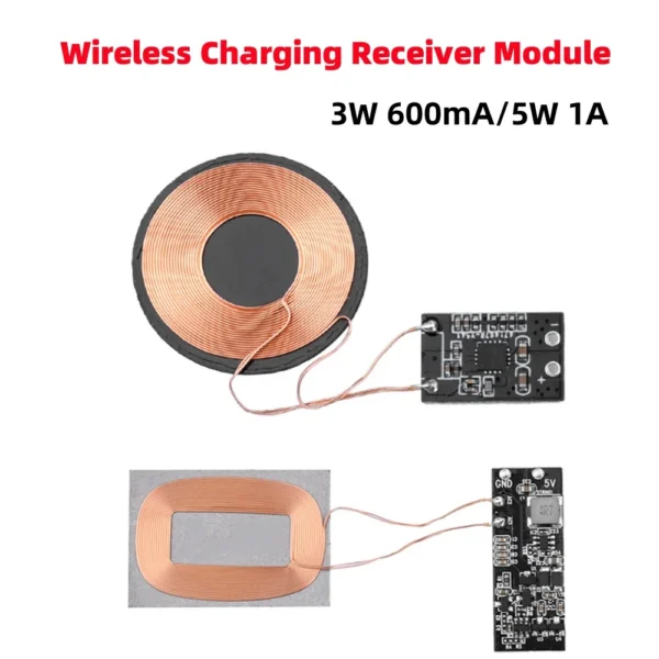 3W 600mA/5W 1A Wireless Charging Receiver Module Small Coil Built-in 5V Charging Wireless Charger PCBA Board
$2.60 – $2.90Price range: $2.60 through $2.90
3W 600mA/5W 1A Wireless Charging Receiver Module Small Coil Built-in 5V Charging Wireless Charger PCBA Board
$2.60 – $2.90Price range: $2.60 through $2.90
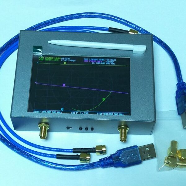 NanoRFE NanoVNA V2 Plus4 Plus5 V2 Plus4 Pro - 4GHz vector network analyzer with 4 inch display
$269.80 – $369.80Price range: $269.80 through $369.80
NanoRFE NanoVNA V2 Plus4 Plus5 V2 Plus4 Pro - 4GHz vector network analyzer with 4 inch display
$269.80 – $369.80Price range: $269.80 through $369.80
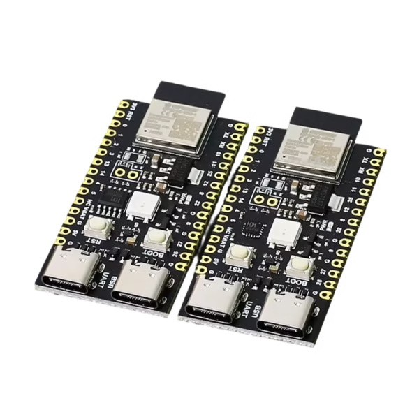 ESP32-H2 Development Board
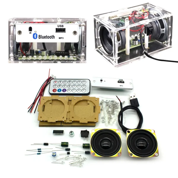 White DIY Electronic Kit Bluetooth Speaker Electronics DIY Soldering Project Kit Teaching Practice Bluetooth Stereo Speaker
$7.90
White DIY Electronic Kit Bluetooth Speaker Electronics DIY Soldering Project Kit Teaching Practice Bluetooth Stereo Speaker
$7.90
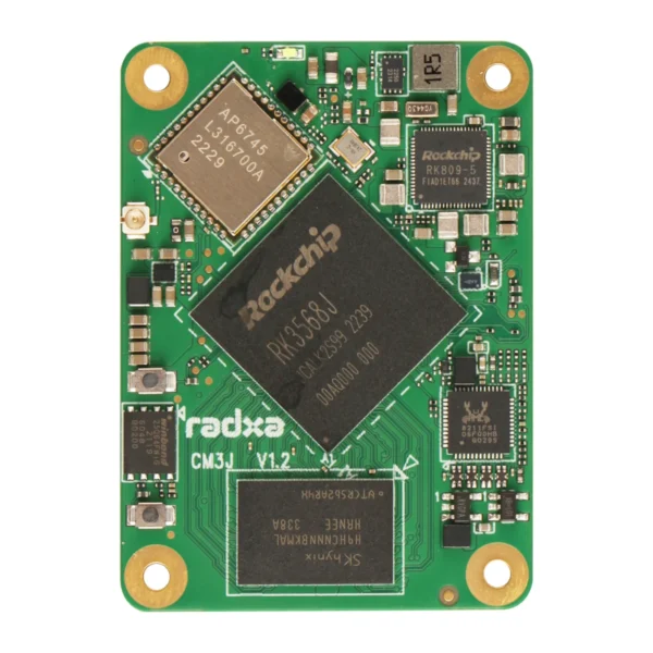 Radxa CM3J RK3568J 4-core CPU, Industrial Compute Module, GPU, NPU, 4K HDMI and 2x100-Pin B2B Connector
$80.50 – $148.90Price range: $80.50 through $148.90
Radxa CM3J RK3568J 4-core CPU, Industrial Compute Module, GPU, NPU, 4K HDMI and 2x100-Pin B2B Connector
$80.50 – $148.90Price range: $80.50 through $148.90