For Hardware Engineering Directors and Supply Chain VPs in the AI sector, the year 2026 presents a brutal paradox. While silicon roadmaps for next-generation AI accelerators (targeting 224G PAM4 and NVLink 6 architectures) are advancing on schedule, the physical interconnects required to support them are caught in a severe supply chain bottleneck.
The epicenter of this crisis is M9 Extreme Low Loss (ELL) Copper Clad Laminate (CCL) and its associated HVLP4 (Hyper Very Low Profile) copper foils. As hyperscale data center builders aggressively hoard advanced materials to build out AI training clusters, mid-tier OEMs, telecom providers, and AI hardware startups are being squeezed out, facing exorbitant spot-market premiums, 20+ week lead times, and catastrophic project delays.
However, the raw cost of the laminate is only half the story. The true margin-killers in 2026 AI hardware projects are the hidden manufacturing inefficiencies and supply chain mismanagement that occur after the materials are procured. This guide provides an unfiltered, factory-floor perspective on the 2026 PCB supply chain, exposes the hidden cost overruns that destroy hardware budgets, and outlines a strategic playbook to secure your production roadmap.
The 2026 AI PCB Supply Chain Reality
Part 1: The Anatomy of the M9 Material Crisis
To navigate the 2026 supply chain, you must first understand why M9 materials (and equivalents like Panasonic Megtron 8/9, Isola Tachyon 100G, or AGC HL8700) are so fiercely constrained. The shortage is not merely a matter of factory capacity; it is a fundamental upstream chemical and metallurgical bottleneck.
1. The HVLP4 Copper Foil Monopoly
At 112Gbps and 224Gbps PAM4 signaling, the "skin effect" forces high-frequency signals to travel exclusively on the outer 1 to 2 microns of the copper trace. Standard roughened copper acts like a mountain range, causing massive insertion loss. To solve this, AI PCBs mandate HVLP4 (Hyper Very Low Profile) foil, which is mirror-smooth.
- The Reality: Only a handful of specialized metallurgy firms in Japan and Europe possess the proprietary electroplating baths and slow-deposition machinery required to produce HVLP4 foil at scale. When top-tier AI silicon vendors lock in multi-year contracts for this foil, the open market simply dries up.
2. The "AI Siphon" Effect
Hyperscalers are not just buying M9 laminates; they are buying entire factory allocations. A 40-layer AI orthogonal backplane consumes 5 to 8 times more sequential lamination machine-hours and UV laser-drilling time than a standard enterprise board. Fabricators are prioritizing these high-margin, high-volume AI contracts, leaving mid-volume medical, aerospace, and edge-AI projects fighting for secondary machine time.
Part 2: The 3 Hidden Cost Overruns Killing AI PCB Margins
Many procurement teams focus obsessively on negotiating the "price per square meter" of the CCL, completely ignoring the hidden Total Cost of Ownership (TCO) traps that inflate the final cost of the assembled PCBA.
Overrun 1: The Panel Utilization Tax on Exotic Laminates
CCL is manufactured and fabricated in standard sheet sizes (e.g., 18x24, 21x24, or 24x36 inches). If your hardware engineering team designs an AI baseboard with awkward dimensions that do not nest efficiently into these standard sheets, you might only achieve 60% to 65% panel utilization.
- The Financial Impact: On a standard FR-4 board, throwing away 35% of the panel as routed scrap is a minor annoyance. On a $600/sheet M9 Ultra-Low Loss laminate, that 35% scrap represents a massive, hidden tax on your BOM. Engineering must collaborate with the fabricator’s CAM (Computer-Aided Manufacturing) team during the layout phase to optimize board dimensions for maximum yield.
Overrun 2: The Prepreg Cold-Chain and Shelf-Life Trap
High-speed prepregs (the "glue" layers in multilayer stack-ups) are highly reactive. They have strict shelf lives (often 3 to 6 months) and require continuous, monitored cold-chain storage.
- The Pain Point: Budget fabricators or unauthorized brokers often buy M9 prepreg in bulk and store it improperly, or let it age in the warehouse to save money. When aged prepreg is used, the resin undergoes advanced cross-linking. During the 260°C SMT reflow process, the resin cannot flow properly, resulting in measling, resin starvation, and catastrophic inner-layer delamination. You don't just lose the cost of the bare board; you scrap a fully populated, $15,000 AI server module.
Overrun 3: The "Over-Specification" Penalty
Fear of signal integrity (SI) failures often leads junior SI engineers to specify top-tier M9 materials for every single layer of a 30-layer board.
- The DFM Reality: Only the specific layers routing 112G/224G differential pairs require M9. The power, ground, and low-speed GPIO layers can safely utilize mid-loss or high-Tg FR-4 materials. Failing to implement a Hybrid Stack-up artificially inflates your CCL BOM cost by up to 40% without providing any measurable electrical benefit.
Part 3: The Grey Market Danger (A Warning to Procurement)
Desperation to meet NPI (New Product Introduction) deadlines drives many hardware teams into the arms of unauthorized, "grey market" PCB brokers. This is a fatal error for AI hardware.
Grey market brokers often source M9 laminates from secondary channels where the chain of custody is broken. You may receive materials that are counterfeit, mislabeled, or, most commonly, expired. Furthermore, M9 materials require specialized Plasma Desmear processes to ensure the ultra-smooth HVLP4 copper adheres to the resin. Grey-market or tier-3 fabricators lack plasma equipment and use standard chemical desmear, guaranteeing that your HVLP inner layers will blister and delaminate during SMT assembly.
In the realm of high-speed AI hardware, Trustworthiness and Authorized Chain of Custody are non-negotiable. You must partner with manufacturers who buy directly from authorized laminate distributors and maintain strict, audited climate-controlled warehousing.
Part 4: The Strategic Playbook: How to Secure Allocations and Protect Margins
To insulate your 2026 AI hardware roadmap from supply chain volatility, engineering and procurement teams must break down their silos and adopt a unified, proactive manufacturing strategy.
Strategy 1: Implement DFM-Driven Hybrid Stack-Ups
Before you lock in your BOM, your PCB stack-up must be audited for cost-efficiency without sacrificing signal integrity. By partnering with a manufacturer that offers deep engineering integration, you can strategically place expensive HVLP/M9 materials only on critical high-speed signal layers, while utilizing cost-effective mid-loss materials for power and ground planes. This requires advanced CAM engineering to manage the Z-axis CTE (Coefficient of Thermal Expansion) mismatch between the different materials, preventing board warpage during lamination.
Strategy 2: Unify Fab and Assembly via Turnkey PCBA
The greatest risk to an M9 high-layer-count board occurs during the SMT assembly phase. These thick, dense boards act as massive heat sinks and are highly prone to thermal warpage during reflow. If your bare board fabricator and your assembly house are separate entities, the critical thermal warpage data is lost in translation, resulting in "head-in-pillow" BGA solder defects.
By leveraging comprehensive Turnkey PCB Assembly Manufacturing Services, you unify the entire production lifecycle. Our SMT engineering team receives the exact lamination data, CTE profiles, and warpage metrics from the bare board fabrication floor. We then design custom reflow pallets and precisely tuned thermal profiles specifically tailored to your exotic M9 stack-up. Furthermore, our turnkey model ensures that your high-speed prepregs are stored in our certified cold-chain facilities and kitted exactly when needed, eliminating shelf-life expiration waste.
Strategy 3: Shift to ODM/OEM Bulk Hedging
Relying on the spot market for M9 laminates and HVLP4 foils in 2026 is a guaranteed path to NPI delays. You must transition to a contract-based model. By initiating a strategic ODM/OEM Bulk Inquiry, enterprise clients can leverage our aggregate purchasing power. We secure long-term, priority allocations with top-tier laminate suppliers (like Panasonic, Isola, and AGC), lock in baseline pricing against volatile petrochemical indexes, and guarantee dedicated machine time on sequential lamination presses and UV laser drills. This transforms your PCB supply chain from a daily vulnerability into a predictable, hedged asset.
FAQ: 2026 PCB Supply Chain & M9 Materials
Q: Why are M9 and Ultra-Low Loss PCB laminates facing 20+ week lead times in 2026?
A: The "AI Siphon" effect. The exponential demand for AI server clusters and 800G/1.6T networking has consumed the majority of global production capacity for specialized hydrocarbon resins and HVLP4 copper foils. Hyperscalers are locking up multi-year contracts, leaving mid-tier OEMs facing severe allocation constraints on the open market.
Q: What is a "Hybrid Stack-up" and how does it reduce AI PCB costs?
A: A hybrid stack-up uses expensive M9 Ultra-Low Loss materials only on the specific inner layers routing 112G/224G high-speed signals, while using more cost-effective mid-loss or high-Tg materials for power, ground, and low-speed layers. This maintains signal integrity while drastically reducing the overall CCL BOM cost and mitigating material shortages.
Q: Why is buying M9 prepreg from the "grey market" dangerous for AI hardware?
A: High-speed prepregs have strict shelf lives (3-6 months) and require continuous cold-chain storage. Grey market brokers often sell expired or improperly stored materials. When degraded resins undergo 260°C SMT reflow, they fail to bond properly, causing catastrophic inner-layer delamination, measling, and the scrapping of highly expensive, fully populated AI assemblies.
Q: How does Turnkey PCBA prevent cost overruns on high-layer AI boards?
A: High-layer count M9 boards are highly susceptible to thermal warpage during SMT reflow. A turnkey partner unifies bare board fabrication and assembly, using exact lamination and CTE data to engineer custom SMT reflow profiles and pallets. This prevents BGA pad cratering, ensures first-pass yield, and eliminates the financial waste of scrapped, populated boards.
Engineering Certainty in a Volatile Market
The PCB supply chain realities of 2026 represent a permanent structural shift in the hardware manufacturing landscape. The days of treating advanced AI laminates as a cheap, easily swappable commodity are over. Today, M9 CCL and HVLP4 foils are highly engineered, geopolitically sensitive, and fiercely contested resources.
Winning in the AI hardware space requires breaking down the silos between electrical engineering, signal integrity, and supply chain procurement. By optimizing stack-ups for panel utilization, implementing hybrid material designs, avoiding the grey market, and securing long-term ODM/OEM partnerships, you can insulate your product margins from upstream volatility and guarantee your hardware ships on time.
Ready to bulletproof your 2026 AI hardware BOM and secure your supply chain? Stop leaving your margins and NPI timelines to the mercy of the spot market and fragmented vendors. Submit your ODM/OEM bulk inquiry today to lock in priority M9/HVLP4 allocations, hedge against material inflation, and secure dedicated manufacturing capacity. Alternatively, explore our Turnkey PCB Assembly and DFM Services to engineer the cost out of your high-speed stack-ups, protect your materials via certified cold-chain kitting, and ensure flawless SMT yields from prototype to mass production.

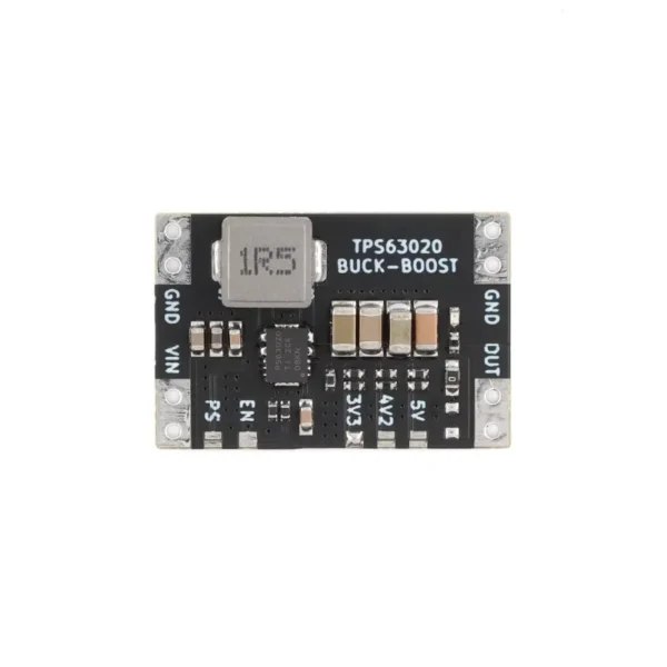 TPS63020 USB Auto Boost Buck Power Module 3.3V/4.2V/5V MCU Power Supply
$2.00
TPS63020 USB Auto Boost Buck Power Module 3.3V/4.2V/5V MCU Power Supply
$2.00
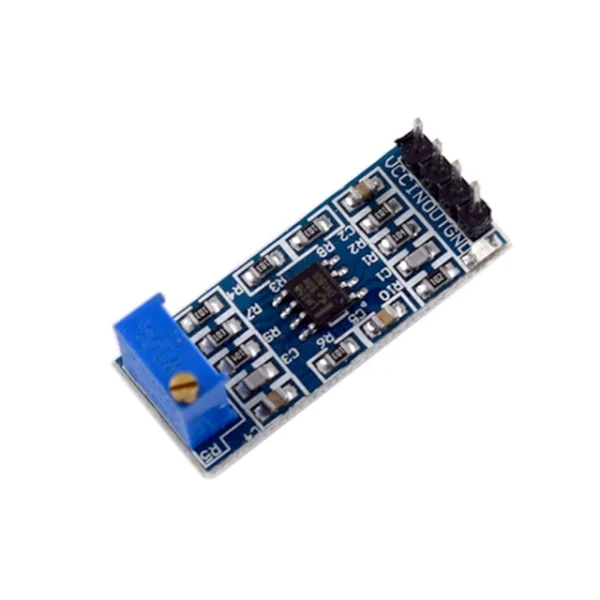 LM358 100 Times Gain Signal Amplification Amplifier Operational Amplifier Module 5V-12V Hot Sale
$2.20
LM358 100 Times Gain Signal Amplification Amplifier Operational Amplifier Module 5V-12V Hot Sale
$2.20
 Mini Handheld Simple Metal Detector DIY Electronic Kit Electronic Components Soldering Assembly School Fun Welding Training Kit
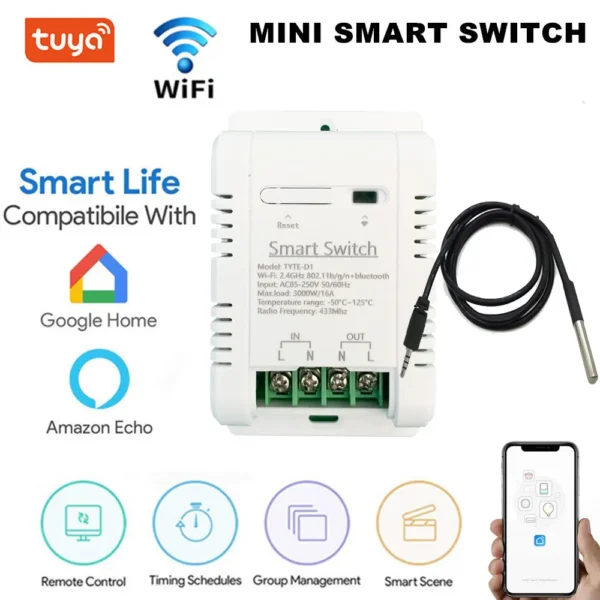 Tuya TH-16 Smart Wifi Switch 16A/3000W Monitoring Temperature Sensor RF433 remote Control Compatible with Alexa Google Home
$12.90 – $15.90Price range: $12.90 through $15.90
Tuya TH-16 Smart Wifi Switch 16A/3000W Monitoring Temperature Sensor RF433 remote Control Compatible with Alexa Google Home
$12.90 – $15.90Price range: $12.90 through $15.90
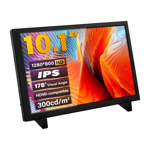 10.1 Inch 1280x800 Touch Screen IPS LCD for Computer Monitor for Switch Xbox 360 HDMI-compatible Display for Raspberry Pi