Beyond the Basics: What is a Multilayer PCB and Why Does It Matter?
A Multilayer Printed Circuit Board (PCB) is not simply a thicker version of a double-sided board. It is a precisely engineered, multi-layered sandwich of conductive copper foils and insulating dielectric materials (such as FR-4, polyimide, or high-frequency laminates), bonded together under high heat and pressure.
While single- and double-layer boards suffice for simple circuits, the miniaturization of modern electronics demands more. Multilayer PCBs (typically ranging from 4 to 30+ layers) allow designers to dedicate specific layers to ground planes, power distribution, and high-speed signal routing. This architecture drastically reduces electromagnetic interference (EMI), improves signal integrity, and allows for a smaller overall footprint.
However, from a manufacturing and procurement standpoint, the complexity of multilayer PCBs introduces significant risks. A minor error in stack-up design, material selection, or lamination can lead to catastrophic field failures. Understanding these nuances is the first step toward building a reliable electronic product.
The Anatomy of a Multilayer PCB: Engineering Implications
To make informed design and sourcing decisions, you must understand how a multilayer PCB is constructed. Each layer serves a critical function, and the interaction between them dictates the board’s reliability:
- Inner Core Layers: The foundation. These are typically double-sided copper-clad laminates. For high-reliability applications, the choice of core material (e.g., standard FR-4 vs. High-Tg FR-4) determines the board’s ability to withstand thermal stress during assembly and operation.
- Prepreg (Bonding Sheets): Uncured fiberglass cloth impregnated with resin. During the lamination process, the prepreg melts, flows, and cures, bonding the core layers and outer copper foils together. Pain Point Alert: Incorrect prepreg selection or improper lamination pressure can cause resin starvation or voids, leading to interlayer delamination.
- Copper Foil: The conductive pathways. Multilayer boards often utilize varying copper weights (e.g., 0.5 oz for inner signal layers to maximize routing space, and 1 oz or 2 oz for outer layers to handle soldering heat and current).
- Blind and Buried Vias: Advanced multilayer boards use these to save space. Blind vias connect an outer layer to one or more inner layers, while buried vias connect only inner layers. This frees up valuable surface area for component placement but requires a more complex (and costly) sequential lamination process.
- Solder Mask and Silkscreen: The outer protective and identification layers, critical for preventing solder bridges and aiding in automated optical inspection (AOI) during assembly.
Advanced Multilayer PCB Technologies for Demanding Applications
Not all multilayer boards are created equal. Depending on your industry, you may require specialized manufacturing capabilities:
- HDI (High-Density Interconnect) Multilayer PCBs: Utilizing microvias (laser-drilled holes typically ≤ 0.15mm), HDI technology allows for finer trace widths and higher component density. Essential for smartphones, wearables, and advanced medical devices.
- High-Frequency / RF Multilayer PCBs: Standard FR-4 has a dielectric constant (Dk) that fluctuates with frequency, causing signal loss. For 5G, radar, and satellite applications, manufacturers must integrate low-loss materials like Rogers or Teflon (PTFE) into the stack-up to maintain strict impedance control.
- Heavy Copper Multilayer PCBs: Featuring copper weights of 3 oz to 6 oz (or more) on inner or outer layers. These are mandatory for power electronics, EV battery management systems, and industrial motor controllers to handle high currents and dissipate heat effectively.
- Rigid-Flex Multilayer PCBs: Combining the durability of rigid multilayer sections with the bendability of polyimide flex circuits. This eliminates the need for bulky connectors and cables, improving reliability in aerospace and dynamic medical equipment.
Top 3 Multilayer PCB Manufacturing Pain Points (And How to Solve Them)
As a hardware developer or supply chain manager, your goal is to avoid costly respins and production delays. Here are the most common multilayer PCB failures and how a professional manufacturing partner mitigates them:
1. Impedance Control Failures
The Pain Point: In high-speed digital or RF designs, a trace impedance deviation of more than ±10% (e.g., targeting 50Ω but achieving 55Ω) causes signal reflection, data corruption, and system crashes.
Our Solution: A competent manufacturer does not just "follow the Gerber files." Their engineering team actively reviews your stack-up, adjusts trace widths and dielectric spacing, and validates the design using field solvers. Post-production, they provide TDR (Time Domain Reflectometry) testing reports on dedicated test coupons to guarantee compliance.
2. Thermal Warpage and Delamination
The Pain Point: During lead-free reflow soldering (which peaks around 260°C), low-quality substrates absorb moisture and expand. This thermal shock can cause the board to warp (making SMT placement impossible) or the layers to delaminate.
Our Solution: Specifying High-Tg (Glass Transition Temperature ≥ 170°C) materials is the first line of defense. Additionally, a rigorous manufacturer will bake the raw materials before lamination to remove moisture and strictly control the thermal profile during the pressing process.
3. DFM (Design for Manufacturability) Blind Spots
The Pain Point: A design may be electrically perfect in CAD but physically unmanufacturable. Common issues include annular rings that are too small for drilling registration, acid traps in trace routing, or insufficient copper balancing leading to warpage.
Our Solution: Never skip the DFM review. A value-added manufacturing partner will run your files through advanced CAM software and provide a detailed, free DFM report before any metal is cut, saving you weeks of delay and thousands of dollars in wasted prototypes.
Why Partner with a Professional Multilayer PCB Manufacturer?
Sourcing a multilayer PCB is not a commodity purchase; it is a strategic supply chain decision. The manufacturer you choose directly impacts your product’s time-to-market, yield rate, and long-term reliability.
We bridge the gap between ambitious engineering designs and scalable manufacturing reality. Our end-to-end capabilities ensure your project succeeds at every stage:
- From Concept to Validated Prototype: Speed is critical in hardware development. We offer rapid-turn multilayer PCB prototyping, coupled with complete turnkey PCB assembly manufacturing. We manage the entire BOM, source authentic components, and deliver fully tested, box-ready units so you can focus on firmware and market validation. Explore our seamless prototype workflow: PCB Prototype & Turnkey PCB Assembly Manufacturing.
- Scalable OEM/ODM Bulk Production: When your design is validated, scaling up requires industrial-grade quality control. We adhere to strict IPC-A-610 Class 2 and Class 3 standards, utilizing Automated Optical Inspection (AOI), X-ray inspection for BGA components, and comprehensive flying probe or fixture testing. We guarantee consistent quality and competitive pricing for high-volume runs. Request a detailed quote for your next large-scale project: OEM/ODM Bulk Inquiry.
- End-to-End Traceability & Compliance: Whether you are building medical devices (ISO 13485), automotive electronics (IATF 16949), or industrial controls, we provide full material traceability and compliance documentation for every batch shipped.
Frequently Asked Questions (FAQ)
Q1: What is the maximum number of layers you can manufacture in a multilayer PCB?
A: We routinely manufacture multilayer PCBs ranging from 4 to 24 layers for standard applications. For highly complex backplane or server applications, we can support up to 30+ layers using advanced sequential lamination and HDI technologies.
Q2: How do you ensure impedance control on multilayer boards?
A: Impedance control is achieved through precise stack-up engineering. We adjust the copper trace width, spacing, and the thickness of the prepreg/core dielectric materials. Every impedance-controlled order includes a TDR (Time Domain Reflectometry) test report to verify the impedance is within your specified tolerance (typically ±10%).
Q3: What is the typical lead time for a multilayer PCB prototype?
A: For standard 4- to 8-layer FR-4 boards, our rapid prototyping lead time is typically 3 to 5 working days. More complex boards (e.g., HDI, heavy copper, or high-frequency materials) may require 7 to 10 days to ensure rigorous quality control. Expedited options are available for critical projects.
Q4: Can you help optimize my multilayer PCB design for lower manufacturing costs?
A: Absolutely. Our engineering team provides a complimentary DFM (Design for Manufacturability) review. We often identify opportunities to simplify the stack-up, optimize panel utilization, or suggest alternative, cost-effective materials that maintain your required performance specifications.
Build Your Next Innovation on a Reliable Foundation
The multilayer PCB is the central nervous system of your electronic device. Compromising on its design, material quality, or manufacturing partner is a direct risk to your product’s performance and your brand’s reputation.
Don’t leave your product’s reliability to chance or outdated manufacturing practices. Whether you need a fast-turn 6-layer prototype to validate your latest IoT architecture, or a trusted, scalable partner for high-volume, high-reliability OEM production, we have the engineering expertise, advanced equipment, and quality management systems to deliver.

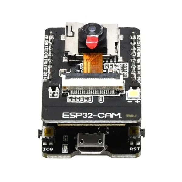 ESP32-CAM-MB MICRO USB ESP32 Serial to WiFi ESP32 CAM Development Board CH340 CH340G 5V Bluetooth+OV2640 Camera
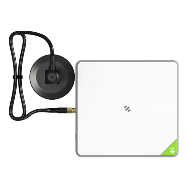 SenseCAP M2 Multi-Platform LoRaWAN Indoor Gateway(SX1302) - AS923
$133.90
SenseCAP M2 Multi-Platform LoRaWAN Indoor Gateway(SX1302) - AS923
$133.90
 Smart WiFi/ZigBee PIR Motion Sensor - Wireless Infrared Security Detector, APP Alerts, Smart Home Burglar Alarm System
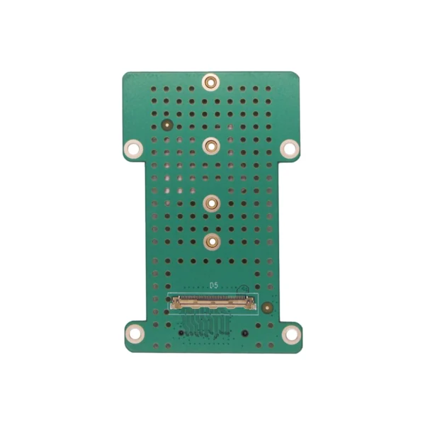 Radxa M.2 extension board for ROCK 4A/4B/4A+/4B+/4SE/3A/5A/3C
$27.90
Radxa M.2 extension board for ROCK 4A/4B/4A+/4B+/4SE/3A/5A/3C
$27.90
 Ultra-Mini Transparent Clock, Calendar & Retro Game Console, 3-in-1 Multi-Function E-Paper Desktop Gadget
$6.90
Ultra-Mini Transparent Clock, Calendar & Retro Game Console, 3-in-1 Multi-Function E-Paper Desktop Gadget
$6.90