Why Solder Composition Dictates PCB Reliability
In modern electronics manufacturing, the transition from Tin-Lead (SnPb) to lead-free solder is no longer optional; it is a strict regulatory requirement driven by the Restriction of Hazardous Substances (RoHS) directive. However, many hardware designers treat solder as a generic commodity, unaware that the specific metallurgical composition directly dictates the mechanical and electrical lifespan of their product.
Lead-free soldering is fundamentally more difficult than traditional soldering. The absence of lead alters the fluid dynamics, thermal conductivity, and metallurgical bonding of the alloy. A minor oversight in alloy selection, surface finish compatibility, or reflow profiling can result in catastrophic field failures, such as cracked solder joints, intermittent connections, or catastrophic delamination.
Understanding the science and manufacturing realities of lead-free solder composition is a mandatory discipline for any hardware team aiming to achieve high first-pass yields and long-term product reliability.
The Chemistry of Reliability: Decoding Lead-Free Alloys
Not all lead-free solders are created equal. The composition is carefully engineered to mimic the desirable properties of tin-lead while eliminating toxicity.
1. SAC305: The Industry Gold Standard
- Composition: 96.5% Tin (Sn), 3.0% Silver (Ag), 0.5% Copper (Cu).
- Why it works: Tin provides the base matrix. Silver significantly improves mechanical strength, fatigue resistance, and wetting characteristics. Copper reduces the dissolution of copper pads and traces into the molten solder, preventing excessive thinning of the PCB during assembly.
- Best For: The vast majority of consumer, industrial, and automotive SMT assembly applications.
2. SAC387 and SAC405: High-Strength Variants
- Composition: Slightly higher Silver (3.8% or 4.0%) and Copper (0.7% or 0.5%).
- Why it works: The increased silver content enhances thermal fatigue resistance and shear strength.
- Best For: High-reliability applications subject to extreme thermal cycling or mechanical vibration, though at a higher material cost due to silver content.
3. SN100C: The Cost-Effective & Wave Soldering Alternative
- Composition: Tin (Sn), 0.7% Copper (Cu), 0.05% Nickel (Ni), and trace Germanium (Ge).
- Why it works: The addition of Nickel suppresses the formation of brittle intermetallic compounds (IMCs) and reduces copper dissolution. Germanium prevents surface oxidation (dross) in the solder pot.
- Best For: Selective wave soldering, through-hole assembly, and cost-sensitive projects where the high cost of silver in SAC alloys is prohibitive.
Top 3 Lead-Free Manufacturing Pain Points (And How We Solve Them)
As a hardware developer or supply chain manager, your goal is to eliminate preventable yield loss. The higher processing temperatures of lead-free solder introduce unique challenges. Here is how a professional manufacturing partner mitigates these risks:
1. Thermal Stress, Warpage, and Delamination
The Pain Point: Lead-free reflow profiles peak at 245°C–260°C, significantly higher than the 215°C–225°C of tin-lead. This extreme heat can cause standard FR-4 substrates to soften, leading to board warpage (which causes SMT misalignment) or Z-axis expansion that cracks plated through-holes (PTH).
Our Solution: We proactively recommend High-Tg (Glass Transition Temperature ≥ 170°C) and low-CTE laminates for lead-free designs. Furthermore, our process engineers design custom, multi-zone reflow profiles with controlled preheat and soak zones to minimize thermal shock and ensure the entire board assembly reaches thermal equilibrium before hitting the peak temperature.
2. Poor Wetting and Solder Voiding
The Pain Point: Lead-free alloys have higher surface tension and do not "flow" or wet copper pads as easily as tin-lead. This often results in insufficient solder fillets, cold joints, or trapped flux gases creating voids (especially under QFN/BGA thermal pads), which severely degrade thermal and mechanical performance.
Our Solution: We combat this through a multi-pronged approach:
- Advanced Flux Chemistry: We utilize no-clean or water-soluble fluxes specifically formulated for lead-free wetting.
- Stencil Optimization: We apply nano-coatings to laser-cut stencils to ensure clean paste release and design segmented (checkerboard) apertures for large thermal pads to allow gases to escape.
- Surface Finish Selection: We guide customers toward highly solderable finishes like ENIG (Electroless Nickel Immersion Gold) or Immersion Silver, which provide a flat, oxidation-resistant surface for the lead-free alloy to bond with.
3. The Silent Killer: Tin Whisker Growth
The Pain Point: Pure tin (and some lead-free alloys) is susceptible to growing microscopic, conductive crystalline structures called "whiskers" over time, driven by compressive stress. In high-voltage or high-density circuits, these whiskers can bridge adjacent pins, causing catastrophic short circuits years after deployment.
Our Solution: For high-reliability sectors (aerospace, medical, automotive), we implement strict anti-whisker protocols. This includes specifying Matte Tin (rather than bright tin) for component finishes, utilizing Nickel (Ni) under-plating as a diffusion barrier, and applying conformal coatings to physically suppress whisker growth.
Lead-Free vs. Leaded Solder: A Technical Decision Matrix
While leaded solder is restricted in commercial production, understanding the trade-offs is vital for legacy system maintenance or specific exempted applications (e.g., certain military/aerospace uses).
The Ultimate DFM Checklist for Lead-Free PCB Assembly
To ensure your design is 100% manufacturable with lead-free processes, your CAD layout must adhere to these industry-proven DFM rules:
- Component Thermal Rating: Verify that every component on your BOM is rated for multiple reflow cycles at a peak temperature of 260°C. Using components rated only for 215°C will result in "popcorn" cracking or internal die damage.
- Thermal Relief Balancing: For through-hole pins connected to large ground planes, use 4-spoke thermal reliefs. Without this, the plane acts as a heat sink, preventing the lead-free solder from reaching liquidus, resulting in a cold, weak joint.
- Pad Size Optimization: Because lead-free solder does not spread as much, slightly increasing the pad size (by 10-15% compared to leaded designs) can improve the solder fillet formation and joint reliability.
- Surface Finish Compatibility: Avoid OSP (Organic Solderability Preservative) for boards that require multiple reflow cycles or have long shelf lives, as the organic layer degrades at lead-free temperatures. Specify ENIG or Immersion Silver for optimal lead-free wetting.
- Via-in-Pad Management: If using lead-free solder, the risk of solder wicking down unfilled vias is higher due to the longer time spent in the liquidus state. Always specify Via-in-Pad Plated Over (VIPPO) for components with pads underneath them.
Why Partner with esp32s.com for Lead-Free PCB Assembly?
Navigating the complexities of lead-free solder composition, thermal profiling, and RoHS compliance requires more than just a standard assembly line. It requires deep metallurgical expertise and rigorous process control. Sourcing bare boards from one vendor and assembly from another often leads to finger-pointing when thermal defects or voiding occur.
You need a unified, accountable partner. At esp32s.com, we bridge the gap between theoretical design and high-yield manufacturing reality:
- Proactive DFM & Material Consultation: Before production begins, our engineering team reviews your Gerber files and BOM. We verify component thermal ratings, validate surface finish compatibility, and optimize your stencil design for lead-free wetting, providing a detailed, free DFM report to eliminate risks before any metal is cut.
- Seamless Prototyping to Turnkey Assembly: Whether you are prototyping a complex IoT device or an industrial controller, our turnkey PCB assembly manufacturing service handles the entire lifecycle. We manage the BOM, source authentic RoHS-compliant components, and execute precision SMT processes with real-time thermal profiling to guarantee perfect, void-free solder joints. Discover how we simplify your workflow: PCB Prototype & Turnkey PCB Assembly Manufacturing.
- Scalable OEM/ODM Bulk Production: When your design is validated, scaling to mass production requires unwavering consistency. We utilize closed-loop Solder Paste Inspection (SPI), 3D Automated Optical Inspection (AOI), and X-ray inspection to verify joint integrity. We guarantee strict RoHS compliance, material traceability, and competitive pricing for high-volume runs. Request a detailed quote for your next large-scale project: OEM/ODM Bulk Inquiry.
FAQ
Q1: What is the most common lead-free solder alloy used in SMT assembly?
A: SAC305 (96.5% Tin, 3.0% Silver, 0.5% Copper) is the undisputed industry standard for SMT reflow assembly due to its optimal balance of melting point, wetting ability, and mechanical reliability.
Q2: Can I mix leaded and lead-free components on the same board?
A: Yes, this is common during transitional phases or when specific components are only available in leaded finishes. However, it requires careful thermal profiling. The reflow profile must be optimized to ensure the lead-free solder reaches its liquidus state (~217°C) without exceeding the maximum temperature rating of the more sensitive leaded components.
Q3: How do you prevent tin whiskers in lead-free PCB assembly?
A: We employ several strategies: specifying Matte Tin (instead of bright tin) for component finishes, using Nickel (Ni) as an under-plating barrier to relieve compressive stress, and offering conformal coating services to physically encapsulate the assembly and prevent whisker propagation.
Q4: Does lead-free PCB assembly cost more than traditional assembly?
A: Slightly, yes. The raw materials (particularly silver in SAC alloys) are more expensive, and the process requires higher-grade laminates, more precise thermal profiling, and advanced inspection (like X-ray for voiding). However, this marginal cost increase is vastly outweighed by the avoidance of regulatory fines, product recalls, and field failures.
Precision Metallurgy is the Foundation of Reliability
Lead-free solder composition is not just a regulatory checkbox; it is a complex metallurgical challenge that directly impacts the thermal, mechanical, and electrical integrity of your electronic product. Ignoring the higher thermal demands and wetting characteristics of alloys like SAC305 is a direct invitation to costly field failures and delayed time-to-market.
By adhering to strict lead-free DFM guidelines and partnering with a manufacturer that possesses the advanced equipment, material science expertise, and rigorous quality controls to handle these alloys, you transform a potential manufacturing bottleneck into a robust, scalable competitive advantage.

 Deauher 32 Watch SE(ESP32S3) 2.4G Wi-Fi TEST V2
$75.90
Deauher 32 Watch SE(ESP32S3) 2.4G Wi-Fi TEST V2
$75.90
 Raspberry Pi Compute Module 4 Antenna Kit Supports 2.4G/5G WiFi Frequency Band For Raspberry Pi CM4 Board
$4.50
Raspberry Pi Compute Module 4 Antenna Kit Supports 2.4G/5G WiFi Frequency Band For Raspberry Pi CM4 Board
$4.50
 Mini Bluetooth Audio Receiver Board Bluetooth 5.0 MP3 Lossless Decoder Board Wireless Stereo Music Module
$2.30
Mini Bluetooth Audio Receiver Board Bluetooth 5.0 MP3 Lossless Decoder Board Wireless Stereo Music Module
$2.30
 Raspberry Pi HQ Camera – M12 mount
$68.90
Raspberry Pi HQ Camera – M12 mount
$68.90
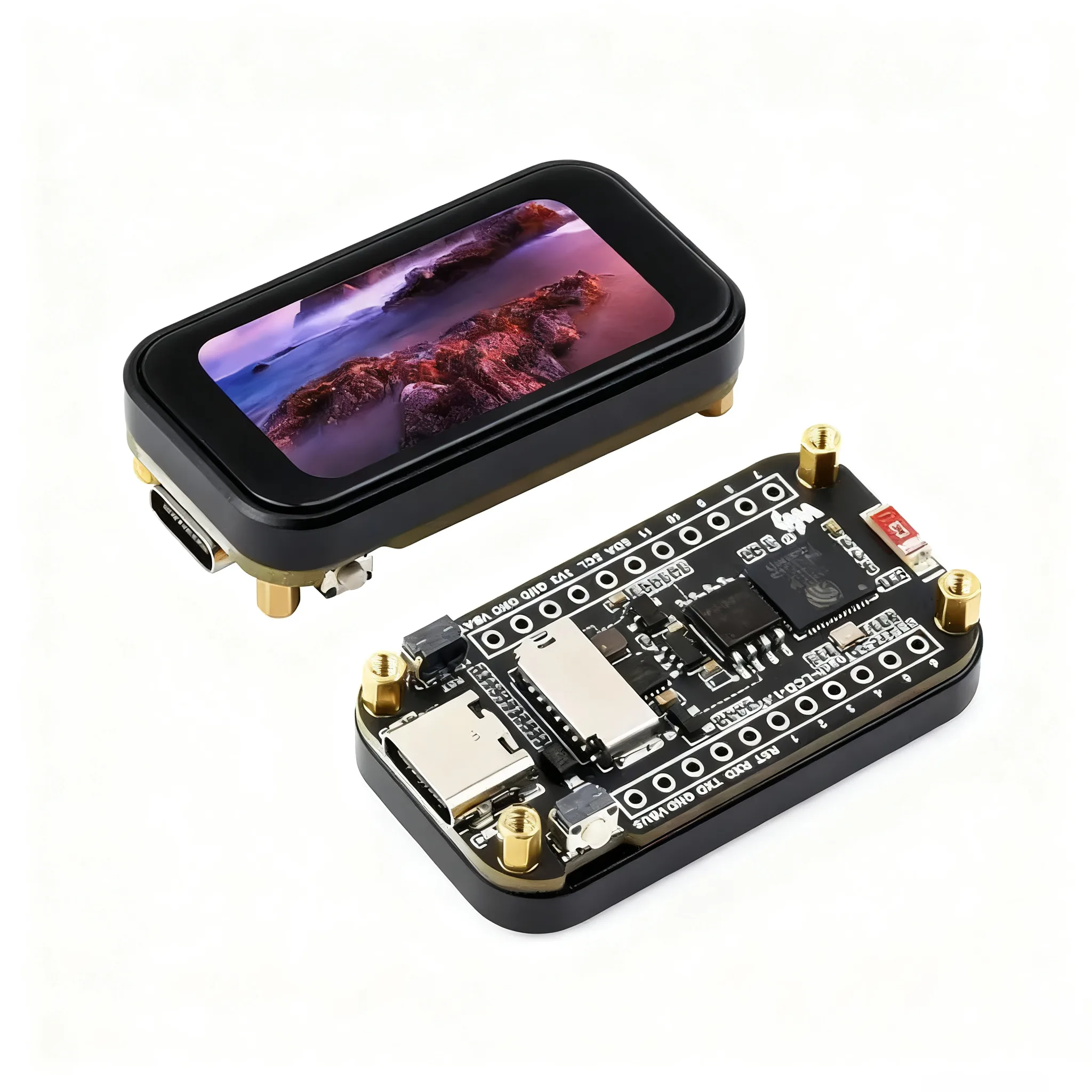 Waveshare ESP32-S3 1.47inch LCD Touch Screen IPS 1.47 inch Display Development Board 172×320 SD AXS5106L JD9853