The era of standard through-hole routing for high-performance compute is dead. As AI silicon evolves—from NVIDIA’s Blackwell architecture to custom Edge AI NPUs and TPUs—the I/O pin counts have exploded. We are routinely seeing Ball Grid Arrays (BGAs) with 2,000 to 4,000+ pins, shrinking to 0.5mm and 0.4mm pitches.
For AI hardware engineers, this creates a brutal physical bottleneck: you simply cannot escape the signals from the BGA footprint using traditional PCB routing.
High-Density Interconnect (HDI) technology is no longer a premium upgrade; it is a mandatory baseline for AI baseboards, switch fabrics, and edge inference modules. However, designing an HDI board for a smartphone is vastly different from designing one for an AI server that must survive 1000A transient currents and 260°C thermal cycling. A single microvia failure or BGA solder wicking defect will scrap a $20,000 prototype and delay your NPI by months.
This guide bypasses basic textbook definitions. Written from the perspective of advanced PCB manufacturing and Signal Integrity (SI) engineering, here are the 10 uncompromising HDI design rules every AI hardware engineer must follow to guarantee first-pass yield and channel compliance.
AI HDI vs. Consumer HDI
The 10 Golden Rules of HDI Design for AI Hardware
Rule 1: Mandate VIPPO for 0.5mm and 0.4mm Pitch BGAs
- The Pain Point: When routing out of a dense BGA, placing a via next to the pad (dog-bone) consumes too much surface space, forcing you to add more layers. Placing the via directly in the pad (Via-in-Pad) saves space, but during SMT reflow, liquid solder wicks down into the hollow microvia, leaving the BGA pad starved of solder (resulting in an open circuit).
- The Rule: For AI ASICs, you must specify VIPPO (Via-in-Pad Plated Over). The fabricator drills the microvia, fills it with specialized epoxy resin, cures it, and plates it flat with copper. This creates a solid, flush surface for the BGA sphere to sit on, eliminating solder wicking and ensuring robust mechanical joints under thermal stress.
Rule 2: Respect the Laser Drill Aspect Ratio Limit
- The Pain Point: AI engineers often stack multiple HDI layers assuming the laser can drill infinitely deep.
- The Manufacturing Reality: CO2 and UV lasers have a strict depth-to-diameter aspect ratio limit, typically 0.75:1 to 1:1. If your dielectric layer is 60µm thick, your microvia diameter cannot be smaller than 60µm. If you violate this, the laser cannot cleanly ablate the bottom copper target, leaving dielectric smear that prevents electrical connection during plating.
- The Rule: Always cross-reference your dielectric thickness (prepreg + core) with the fabricator’s laser minimum diameter. When in doubt, increase the microvia pad diameter to ensure a reliable capture pad.
Rule 3: Stacked vs. Staggered Microvias (The Yield vs. SI Tradeoff)
- The Pain Point: To route deep into a 30-layer AI board, you need multiple HDI build-ups. Staggered vias (offsetting the vias on adjacent layers) are easier to manufacture but consume massive amounts of surface routing space. Stacked vias (drilling directly on top of the buried via below) save space and offer superior Signal Integrity (fewer impedance discontinuities) but are highly prone to Z-axis CTE (Coefficient of Thermal Expansion) separation during reflow.
- The Rule: For 112G/224G PAM4 high-speed differential pairs, stacked microvias are often mandatory to maintain phase alignment and minimize stub length. However, you must partner with a manufacturer capable of advanced copper-filled stacking processes to prevent inter-layer separation. For power and ground routing, use staggered vias to reduce cost and improve structural integrity.
Rule 4: Implement Aggressive Copper Balancing to Prevent Warpage
- The Pain Point: HDI build-up layers are extremely thin. If one side of the board has dense BGA escape routing (heavy copper) and the other side is mostly empty resin, the asymmetric shrinkage during the lamination cooling process will cause severe board warpage. When the board hits the SMT line, the warped BGA footprint will cause "head-in-pillow" solder defects.
- The Rule: Never leave large empty areas on HDI signal layers. Use your CAD tool’s copper balancing (dummy copper filling) features to distribute copper evenly across the panel. Work with your CAM engineer to ensure the copper distribution is symmetrical across the Z-axis.
Rule 5: Mitigate Glass Weave Skew in Thin HDI Dielectrics
- The Pain Point: HDI relies on very thin dielectric layers (e.g., 40µm - 60µm). At these thicknesses, the physical fiberglass bundles are highly prominent relative to the trace width. If a 112G differential pair routes over a glass bundle on the P-trace and resin on the N-trace, the Dk mismatch causes fatal phase skew.
- The Rule: Specify Spread Glass (mechanically flattened glass yarn) for your HDI prepregs to create a homogenous dielectric. Additionally, enforce a 10° to 15° routing angle in your layout constraints to ensure both traces of the pair cross identical glass/resin ratios.
Rule 6: Design Thermal Via Arrays for AI NPU Heat Slugs
- The Pain Point: Edge AI modules and server baseboards generate immense localized heat. The bottom thermal pad (EP) of the AI chip must transfer heat into the inner ground planes. Standard vias are too large and sparse.
- The Rule: Design a dense microvia thermal array directly under the component's thermal slug. Specify that these vias be filled and capped (VIPPO) to prevent solder from flowing away from the thermal pad during SMT, which would otherwise create a massive thermal bottleneck and cause the AI chip to throttle.
Rule 7: Optimize Annular Ring and Registration Tolerances
- The Pain Point: HDI requires sequential lamination (pressing, drilling, and plating multiple times). Every lamination cycle introduces slight material shrinkage and X/Y drift. If your microvia target pad (annular ring) on the inner layer is too small, the laser drill will miss the pad ("breakout"), causing an open circuit.
- The Rule: Do not use minimum CAD annular rings for inner-layer capture pads in HDI stack-ups. Add a DFM margin of at least 1.5 to 2.0 mils to inner-layer target pads to accommodate the cumulative registration drift of a 3-stage or Any-Layer HDI process.
Rule 8: Select Laser-Friendly Dielectric Materials
- The Pain Point: Not all high-speed laminates drill well with lasers. Some ultra-low loss materials are heavily loaded with silica fillers to control CTE. High silica content absorbs CO2 laser energy poorly, resulting in rough, jagged hole walls that cause plating voids and signal scattering.
- The Rule: Consult your PCB manufacturer’s material matrix. Ensure the prepreg selected for your HDI build-up layers is optimized for UV or CO2 laser ablation. Sometimes, a hybrid stack-up using a laser-friendly material for the HDI layers and a specialized low-loss material for the core signal layers is the most reliable approach.
Rule 9: Isolate RF/Analog from Digital HDI Noise
- The Pain Point: Edge AI devices often combine high-speed digital HDI routing (PCIe, MIPI) with sensitive analog sensor inputs or RF antennas on the same compact board. The dense stitching vias and return currents in HDI can easily couple noise into analog traces.
- The Rule: Utilize buried ground planes and dedicated shielding via fences (ground stitching) around RF and analog sections. Keep high-speed digital HDI layers physically separated from analog layers by at least one thick, solid ground core.
Rule 10: Engage in Pre-Layout DFM Collaboration
- The Pain Point: The most expensive mistake an AI hardware team can make is finalizing a 14-layer HDI stack-up in a vacuum, only to have the fabricator reject it 6 weeks later due to impossible aspect ratios or sequential lamination limits.
- The Rule: DFM (Design for Manufacturing) must happen before layout begins. Your engineering team must sit down with the PCB manufacturer’s CAM engineers to lock in the stack-up, material choices, and VIPPO tolerances.
The Yield & Supply Chain Reality: Bridging Design and Manufacturing
Designing a flawless HDI PCB for AI hardware is only 40% of the battle. The other 60% is surviving the manufacturing floor and the SMT assembly process.
HDI boards, particularly those utilizing VIPPO and stacked microvias, are highly sensitive to the thermal stresses of SMT reflow. If your bare board fabricator and your PCBA assembly house are separate entities, the critical thermal warpage data and CTE profiles are often lost in translation. When a BGA fails due to a cracked microvia barrel, the board house blames the assembly house's reflow profile, and the assembly house blames the board house's plating quality. Your product launch stalls.
The Turnkey PCBA Advantage
To eliminate this risk, AI hardware teams must unify fabrication and assembly. By leveraging comprehensive Turnkey PCB Assembly Manufacturing Services, you ensure that the exact lamination data, VIPPO planarity metrics, and thermal mass of your HDI board are fed directly into the SMT engineering team. We design custom reflow pallets and precisely tuned thermal profiles specifically tailored to your HDI stack-up, ensuring that massive AI ASICs and 01005 passives are soldered perfectly on the first pass, preserving the integrity of your microvias.
Securing Exotic Materials via ODM/OEM Partnerships
Furthermore, the specialized materials required for AI HDI—such as Spread Glass, Low-Dk prepregs, and specialized via-fill resins—are subject to severe supply chain constraints and long lead times. Attempting to source these on the spot market for every prototype spin is a recipe for NPI delays.
By initiating a strategic ODM/OEM Bulk Inquiry, enterprise clients can leverage our aggregate purchasing power. We secure long-term allocations for advanced HDI laminates, lock in pricing against volatile commodity indexes, and provide dedicated, climate-controlled warehousing for your via-fill resins and prepregs, ensuring your production schedule is never derailed by material shortages.
HDI PCB Design for AI Hardware
Q: What is VIPPO and why is it required for AI BGA routing?
A: VIPPO stands for Via-in-Pad Plated Over. It is a process where a microvia is drilled directly in the BGA pad, filled with epoxy resin, and plated flat with copper. It is mandatory for 0.5mm and 0.4mm pitch AI chips to prevent solder from wicking down into the hollow via during SMT reflow, which would otherwise cause catastrophic open-circuit solder joints.
Q: What is the maximum aspect ratio for laser-drilled microvias in HDI?
A: The industry standard maximum aspect ratio for CO2 or UV laser-drilled microvias is typically 0.75:1 to 1:1 (depth to diameter). Exceeding this limit prevents the laser from cleanly ablating the bottom copper target, leading to dielectric smear and plating voids.
Q: Are stacked microvias better than staggered microvias for AI servers?
A: For high-speed 112G/224G signals, stacked microvias are preferred because they save routing space and minimize impedance discontinuities (stubs). However, they are more expensive and require advanced manufacturing processes to prevent Z-axis separation during thermal cycling. Staggered vias are better suited for power/ground routing to reduce cost and improve mechanical strength.
Q: How does HDI design affect PCB warpage during SMT?
A: HDI utilizes very thin dielectric layers and sequential lamination, making the board highly susceptible to asymmetric copper shrinkage. If copper is not balanced evenly across the layers, the board will warp, causing "head-in-pillow" BGA solder defects. Strict copper balancing and symmetrical stack-ups are mandatory.
Engineering Reliability at the Micro-Level
In the realm of AI hardware, the macro-performance of your neural network is entirely dependent on the micro-reliability of your PCB interconnects. HDI technology is the only bridge between the silicon and the system, but it is an unforgiving discipline. Ignoring the physics of laser ablation, the chemistry of VIPPO, and the thermal realities of SMT reflow will result in catastrophic yield losses and delayed time-to-market.
Hardware innovators must stop treating HDI layout as a purely digital exercise. It is a physical manufacturing contract. By adhering to these 10 rules and aligning with a manufacturing partner that understands the intersection of advanced fabrication and precision SMT assembly, you can guarantee the reliability of your next-generation AI infrastructure.
Ready to de-risk your AI HDI hardware program? Stop fighting yield issues on the SMT line and start engineering for manufacturing success. Submit your ODM/OEM bulk inquiry today to secure priority access to advanced HDI materials and dedicated sequential lamination capacity. Alternatively, explore our Turnkey PCB Assembly Services to unify your DFM, fabrication, and SMT processes, ensuring your high-density AI channels pass compliance on the very first prototype spin.

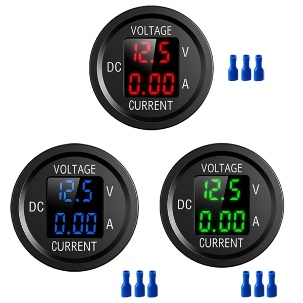 DC 5-48V Car Motorcycle Voltmeter Ammeter Mini Digital Waterproof LED Panel Tester Display Round Volt Meter Gauge For 12V Truck
$6.90
DC 5-48V Car Motorcycle Voltmeter Ammeter Mini Digital Waterproof LED Panel Tester Display Round Volt Meter Gauge For 12V Truck
$6.90
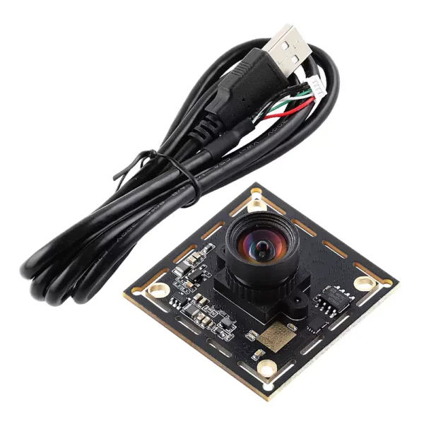 OV9281 USB Industrial Camera Module – Global Shutter, Monochrome, 120fps High-Speed, Driver-Free, Adjustable Field of View
$30.90
OV9281 USB Industrial Camera Module – Global Shutter, Monochrome, 120fps High-Speed, Driver-Free, Adjustable Field of View
$30.90
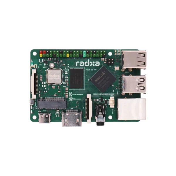 Radxa ROCK 3C RK3566 4-core CPU SBC, GPU, NPU, and HDMI with 4K Output, Single Board Computer
$35.90 – $123.90Price range: $35.90 through $123.90
Radxa ROCK 3C RK3566 4-core CPU SBC, GPU, NPU, and HDMI with 4K Output, Single Board Computer
$35.90 – $123.90Price range: $35.90 through $123.90
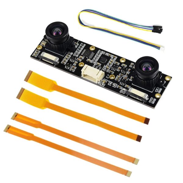 Jetson Nano Camera 8MP IMX219 Binocular Camera Stereo Vision Depth Vision Stereo Camera for Raspberry Pi 5 CM4 Orin
$47.90
Jetson Nano Camera 8MP IMX219 Binocular Camera Stereo Vision Depth Vision Stereo Camera for Raspberry Pi 5 CM4 Orin
$47.90
 1.8-Inch 2.4-Inch TFT Display Screen With Ec11 Rotary Encoder Combination Module SPI Interface LCD Screen Electronic Kit
$6.50 – $6.90Price range: $6.50 through $6.90
1.8-Inch 2.4-Inch TFT Display Screen With Ec11 Rotary Encoder Combination Module SPI Interface LCD Screen Electronic Kit
$6.50 – $6.90Price range: $6.50 through $6.90