In the high-stakes world of AI hardware manufacturing, a single broken drill bit can turn a $15,000, 40-layer server baseboard into scrap metal.
As the industry scales to support architectures like NVIDIA’s Rubin, 800G optical switches, and high-frequency trading platforms, Printed Circuit Boards (PCBs) have become incredibly thick and densely packed. To route 112Gbps and 224Gbps PAM4 signals through 30 to 50+ layers, engineers are forced to utilize extreme high-aspect-ratio vias and exotic, abrasive dielectric materials like Quartz glass and filled PTFE.
For hardware OEMs and signal integrity (SI) engineers, the CAD simulation is only half the battle. The physical reality of AI PCB drilling introduces catastrophic failure modes: drill wander, resin smear, nail-heading, and stub resonance. If your manufacturing partner relies on legacy drilling parameters and standard tungsten carbide tooling, your yield rates will plummet, and your high-speed channels will fail link training.
This guide provides a deep, factory-floor analysis of the mechanical and thermal challenges of drilling next-generation AI PCBs, and how advanced tooling and precision CNC strategies are the only way to guarantee interconnect reliability.
Standard vs. AI PCB Drilling Realities
Part 1: The Physics of the AI Drilling Nightmare
To understand why AI PCBs destroy standard manufacturing processes, we must look at the extreme physical constraints of modern interconnects.
1. The High Aspect Ratio Limit
In a 40-layer AI switch board, the total thickness often exceeds 4.0mm. To escape the dense Ball Grid Arrays (BGAs) of modern AI ASICs, engineers must use via diameters as small as 0.15mm or 0.10mm.
- The Math: A 0.15mm hole drilled through a 4.0mm board creates an aspect ratio of nearly 27:1.
- The Reality: A carbide drill bit with a 0.15mm diameter and a 4.0mm flute length is essentially a microscopic spaghetti noodle. When it plunges into dense fiberglass and copper at 30,000 RPM, it is highly susceptible to drill wander (deflection) and catastrophic snap-breakage. If the drill wanders just 2 mils, it misses the inner-layer capture pad, resulting in an open circuit buried deep inside the board.
2. The Abrasiveness of Exotic Materials
To maintain signal integrity at 112G+, AI PCBs utilize Quartz (Q-Fabric) and specialized Low-DK glass to eliminate glass-weave skew. Furthermore, RF and microwave sections of AI boards use filled PTFE (Teflon) ceramics.
- The Pain Point: Quartz and ceramic-filled PTFE are highly abrasive. A standard tungsten carbide drill bit that can drill 3,000 holes in FR-4 will dull and degrade after just 300 hits in Quartz. A dull bit generates excessive heat, tearing the copper foil and causing nail-heading (where the inner layer copper is pushed away from the hole wall, creating a void that leads to interconnect separation during thermal cycling).
Part 2: The 4 Fatal Drilling Defects (And How They Kill Signal Integrity)
When hardware startups send their complex designs to tier-2 board houses, they frequently encounter yield failures that cannot be detected by standard electrical testing. Here are the hidden defects caused by poor drilling practices.
Defect 1: Resin Smear and Interconnect Separation
The high-speed friction of a mechanical drill bit generates intense localized heat. In high-Tg and exotic AI laminates, this heat melts the resin, smearing it across the inner-layer copper pads.
- The Consequence: If the chemical desmear process cannot completely dissolve this glass/resin smear, the subsequent electroless copper plating will not bond to the inner layer. During SMT reflow, the thermal expansion causes the via barrel to pull away from the pad, creating a microscopic crack that fails only when the server is under heavy AI compute loads.
Defect 2: The Back-Drilling Stub Resonance
At 112Gbps PAM4, the unused portion of a plated through-hole (PTH) via acts as an antenna, reflecting high-frequency energy back into the signal path. This "stub resonance" collapses the signal eye diagram.
- The Solution: Back-drilling (using a slightly larger drill bit to mill out the unused copper stub from the opposite side of the board).
- The Challenge: The depth tolerance for back-drilling in 2026 AI boards is ±1 mil. If the CNC machine drills 2 mils too shallow, the stub remains and ruins the signal. If it drills 2 mils too deep, it severs an active high-speed trace on an adjacent layer, destroying the board.
Defect 3: Microvia Cratering in HDI
AI baseboards rely heavily on Any-Layer HDI (High-Density Interconnect) microvias to route BGA escapes. Mechanical drilling is too large for these features, requiring laser drilling. However, improper laser energy settings on Low-DK glass can cause "cratering"—where the glass fibers protrude above the resin, preventing the subsequent copper plating from forming a reliable, flat base.
Part 3: Advanced Tooling & CNC Strategies: How We Ensure Quality
Overcoming these physical limitations requires massive capital investment in advanced drilling technology and rigorous process control. Here is how a specialized high-layer count PCB manufacturer guarantees yield.
1. Advanced Carbide Geometries and Coatings
We do not use off-the-shelf micro-drills for AI PCBs. We utilize ultra-fine micro-grain tungsten carbide bits with specialized TiAlN (Titanium Aluminum Nitride) or Diamond-Like Carbon (DLC) coatings. These coatings reduce friction, dissipate heat, and extend tool life when drilling abrasive Quartz and M9 laminates. Furthermore, the flute geometry is optimized for "peck drilling" cycles, allowing the bit to retract slightly to clear swarf (debris) and prevent bit breakage in 25:1 aspect ratio holes.
2. AI-Driven Depth Sensing for Back-Drilling
To achieve the ±1 mil tolerance required for 224G back-drilling, legacy CNC machines relying on Z-axis mechanical limits are insufficient. We utilize drilling machines equipped with piezoelectric and acoustic depth sensors. The machine dynamically measures the exact thickness of the board at every single hole location, automatically compensating for microscopic warpage or copper thickness variations, ensuring the stub is removed perfectly every time without damaging adjacent layers.
3. UV Laser Drilling for HDI Microvias
For the ultra-dense BGA escape routes found on AI GPU baseboards, mechanical drills are too large. We deploy UV Laser Drilling systems (355nm wavelength). Unlike CO2 lasers that burn through material via heat, UV lasers break the molecular bonds of the dielectric and copper cleanly ("cold ablation"). This creates perfectly cylindrical microvias with zero thermal damage to the surrounding HVLP copper foil, ensuring perfect seed-layer adhesion for subsequent pulse plating.
4. Automated 3D X-Ray and TDR Validation
You cannot trust what you cannot see. Post-drilling and post-plating, we utilize 3D X-Ray inspection to verify the internal alignment of high-aspect-ratio vias and the exact depth of back-drilled stubs. Furthermore, Time Domain Reflectometry (TDR) is used to test the impedance of the vias, ensuring that the drilling and plating processes have not introduced any capacitive or inductive discontinuities that would degrade 112G signals.
Part 4: The Supply Chain & Turnkey Reality
The precision required to drill a 40-layer AI PCB is inextricably linked to the SMT assembly process. If the mechanical stress of high-aspect-ratio drilling introduces micro-fractures or latent warpage into the board, it will not survive the 260°C lead-free reflow process when massive AI heat sinks and BGA components are attached.
This is why hardware OEMs are rapidly abandoning fragmented supply chains. When the bare board fabricator and the assembly house are separate entities, drilling defects are often masked until the final functional test, resulting in weeks of finger-pointing and delayed product launches.
The Strategic Advantage of Unified Manufacturing
By leveraging comprehensive Turnkey PCB Assembly and Manufacturing Services, you unify the drilling, plating, and SMT processes under one rigorous quality management system. Our SMT engineers collaborate with our CNC drilling team to design custom reflow pallets that support the specific mechanical stress points of high-aspect-ratio via fields, ensuring first-pass yield and protecting your multi-million-dollar hardware investments.
Furthermore, the exotic tooling and materials required for AI PCBs are subject to severe supply chain constraints. By initiating a consolidated ODM/OEM Bulk Inquiry, enterprise clients can secure priority access to specialized coated micro-drills, UV laser time, and M9/Quartz laminates, ensuring your production schedule is never derailed by tooling shortages.
FAQ: AI PCB Drilling & Manufacturing
Q: What is the maximum aspect ratio for mechanical drilling in AI PCBs?
A: While standard PCBs handle 10:1 aspect ratios, advanced AI server PCBs routinely require 20:1 to 30:1 aspect ratios (e.g., a 0.15mm hole through a 4.5mm board). This requires specialized CNC machines, peck-drilling cycles, and ultra-fine coated carbide tooling to prevent drill wander and breakage.
Q: Why is back-drilling critical for 112G and 224G PCBs?
A: At data rates above 56Gbps, the unused portion of a plated through-hole (the "stub") acts as an antenna, causing signal reflection and resonance that destroys the PAM4 eye diagram. Back-drilling removes this stub, but requires extreme depth control (±1 mil tolerance) to avoid damaging adjacent high-speed signal layers.
Q: How do manufacturers drill Quartz and Low-DK glass without breaking bits?
A: Quartz and ceramic-filled PTFE are highly abrasive and dull standard carbide bits rapidly. Specialized manufacturers use ultra-fine micro-grain carbide with Diamond-Like Carbon (DLC) coatings, combined with optimized spindle speeds and peck-drilling cycles to clear debris and reduce thermal friction.
Q: What is the difference between CO2 and UV laser drilling for HDI microvias?
A: CO2 lasers use thermal energy to burn through dielectrics, which can cause thermal damage and smearing on advanced low-loss materials. UV lasers (355nm) use "cold ablation" to break molecular bonds, creating clean, perfectly cylindrical microvias essential for reliable copper plating in high-density AI BGA escape routes.
Precision is the Only Metric That Matters
In the era of AI and hyperscale computing, the physical interconnect is the ultimate bottleneck. You can design the most sophisticated 112G/224G routing architecture in the world, but if your manufacturing partner cannot reliably drill a 25:1 aspect ratio via through abrasive Quartz glass, or back-drill a stub with ±1 mil precision, your hardware will fail.
Drilling in AI PCBs is not a commodity process; it is a highly specialized discipline requiring advanced metallurgy, laser physics, and dynamic CNC control. Hardware OEMs that ignore the realities of drill wander, resin smear, and tool wear will face catastrophic yield losses and delayed time-to-market.
Ready to engineer reliability into your AI infrastructure? Stop risking your high-layer count designs on legacy manufacturing processes. Submit your ODM/OEM bulk inquiry today to secure capacity for advanced drilling and exotic materials, or explore our Turnkey PCB Assembly Services to ensure your critical AI interconnects are fabricated, drilled, and assembled with world-class precision and guaranteed yield.

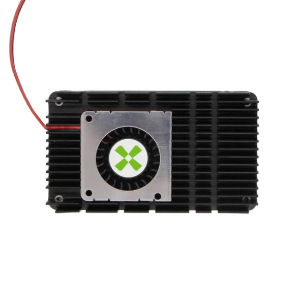 Radxa Heatsink 7012B, Designed for Radxa CM3I, Adjustable Fan Speed, Easy to Install and Remove.
$13.90
Radxa Heatsink 7012B, Designed for Radxa CM3I, Adjustable Fan Speed, Easy to Install and Remove.
$13.90
 ESP32-S3 1.32inch AMOLED Round Touch Display Development Board, 466×466 Pixels, QSPI Interface, Supports Wi-Fi and Bluetooth 5
$25.90
ESP32-S3 1.32inch AMOLED Round Touch Display Development Board, 466×466 Pixels, QSPI Interface, Supports Wi-Fi and Bluetooth 5
$25.90
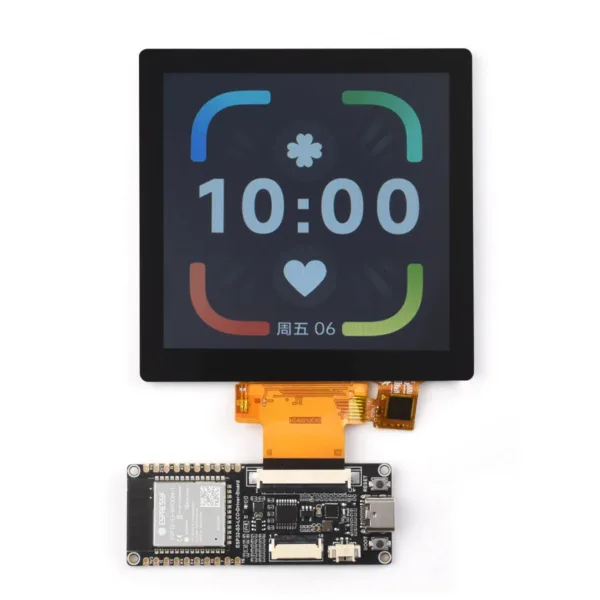 ESP32-S3 RGB LCD Driver Board 2.1inch 2.8inch 4.0inch RGB Round Touch Display Module WiFi & Bluetooth HMI LVGL GUI Development
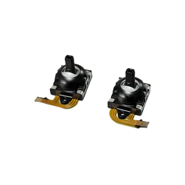 1Pair K-Silver Left Right Hall Joystick for SONY PS VR2 Sense PlaySation Portal Controller Handle Hall Operating Direction Stick
$6.90
1Pair K-Silver Left Right Hall Joystick for SONY PS VR2 Sense PlaySation Portal Controller Handle Hall Operating Direction Stick
$6.90
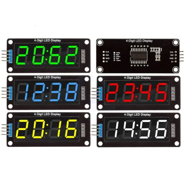 HT16K33 LED Display Module for Arduino 4 Digit 7 Segment 0.56 inch Time Clock Indicator Tube Module Red Blue Green Yellow White
$4.90
HT16K33 LED Display Module for Arduino 4 Digit 7 Segment 0.56 inch Time Clock Indicator Tube Module Red Blue Green Yellow White
$4.90