The AI hardware landscape is undergoing a tectonic shift. Driven by the exorbitant costs and supply chain monopolies of merchant GPUs, hyperscalers (Google, AWS, Meta, Microsoft) and aggressive AI startups are pivoting massively toward Custom ASICs (Application-Specific Integrated Circuits) like TPUs, Trainium, and MTIA. Industry data reflects this explosion: the custom AI accelerator segment is experiencing a staggering 40% Year-over-Year (YoY) growth.
But for Hardware VPs, Lead Signal Integrity (SI) Engineers, and NPI (New Product Introduction) Managers, this silicon renaissance is colliding with a brutal physical bottleneck: The Printed Circuit Board.
Designing a baseboard for a custom hyperscaler ASIC is fundamentally different from designing for a standardized GPU module. ASICs utilize massive 2.5D/3D packaging, extreme low-voltage power delivery, and proprietary high-bandwidth interconnects. The PCB is no longer just a passive interconnect; it is an extension of the silicon interposer.
Drawing from the hard-won battle scars of recent NPI cycles, this guide bypasses surface-level theory. We expose the 4 critical manufacturing realities of designing custom PCBs for hyperscaler ASICs, and provide the actionable DFM (Design for Manufacturing) playbooks required to protect your multi-million-dollar silicon investments.
The Hyperscaler ASIC PCB Paradigm
- The Market Driver: A 40% YoY surge in custom AI silicon is forcing a shift from standard sequential lamination to Any-Layer HDI and CoWoP (Chip-on-Wafer-on-PCB) architectures.
- The Core Pain Point: ASICs demand 0.35mm BGA pitches and ultra-low core voltages (0.5V), making standard PCB routing and power delivery networks (PDN) physically obsolete.
- The Fatal NPI Killer: Z-axis CTE (Coefficient of Thermal Expansion) mismatch between 40+ layer M9 laminates and massive 2.5D interposers, leading to catastrophic BGA pad cratering during SMT reflow.
- The Strategic Fix: Unifying bare board fabrication and SMT assembly via Turnkey PCBA and securing upstream material allocations via ODM/OEM partnerships.
Lesson 1: The PDN Reality Check – Heavy Copper vs. Lamination Warpage
Custom ASICs are designed for maximum compute-per-watt efficiency. To achieve this, silicon architects push core voltages down to ultra-low levels (e.g., 0.5V to 0.7V) while drawing massive, continuous currents. At 0.5V, even a few millivolts of DC resistance (IR Drop) across the PCB traces will cause the silicon to throttle or crash.
The Engineering Pain Point
To mitigate IR drop, hardware teams are forced to specify 3oz to 6oz heavy copper for dedicated power and ground layers. However, integrating thick, rigid heavy copper layers with ultra-thin, delicate M9 Ultra-Low Loss signal layers creates a massive Coefficient of Thermal Expansion (CTE) mismatch. During the sequential lamination process, the thick copper and the exotic resin expand and contract at vastly different rates. The result? Severe internal board warpage, resin starvation, and micro-cracking in the high-aspect-ratio vias.
The DFM Solution: Hybrid Stack-Up Harmonization
You cannot simply "add more copper" without consequences. Advanced PCB manufacturers utilize 3D thermomechanical simulation during the pre-layout DFM phase. We help engineering teams implement hybrid stack-ups, strategically balancing heavy copper power planes with symmetrical, dummy-copper-filled signal layers to neutralize Z-axis stress. Furthermore, we utilize specialized low-flow prepregs and multi-stage lamination cooling cycles to "freeze" the resin matrix uniformly, ensuring the board remains flat enough to survive the SMT pick-and-place process.
Lesson 2: The HDI & Microvia Gauntlet – Escaping the 0.35mm BGA
Hyperscaler ASICs bypass standard PCIe bottlenecks by utilizing massive 2.5D/3D packaging (like CoWoS or the emerging CoWoP). A next-gen AI ASIC can feature 10,000+ I/O pins on a single package, shrinking to 0.4mm and 0.35mm BGA pitches.
The Engineering Pain Point
Standard mechanical drilling and "dog-bone" trace routing physically cannot escape the signals from a 0.35mm pitch footprint without shorting. ASIC baseboards mandate Any-Layer HDI (High-Density Interconnect) technology. This requires laser-drilled microvias, stacked via structures, and VIPPO (Via-in-Pad Plated Over).
- The Manufacturing Trap: Stacked microvias (drilling directly on top of a buried via) are highly susceptible to Z-axis separation during the 260°C SMT reflow process. If the fabricator’s copper fill and cap plating processes are not flawless, the vias will crack internally, destroying the multi-million-dollar ASIC module. Furthermore, if VIPPO is not planarized perfectly, the BGA spheres will suffer from "Head-in-Pillow" (HiP) solder defects.
The DFM Solution: Advanced Laser Ablation & VIPPO Mastery
Fabricating ASIC baseboards requires massive CapEx in UV Laser Drilling systems. Unlike CO2 lasers that burn through material via heat (causing thermal damage to Low-DK glass), UV lasers use "cold ablation" to break molecular bonds, creating perfectly cylindrical microvias. Combined with automated optical inspection (AOI) and 3D X-Ray validation of the epoxy via-fill process, we guarantee that your HDI escape routes maintain structural integrity and signal continuity through multiple thermal cycles.
Lesson 3: The Material Science Bottleneck – M9, HVLP4, and the Supply Chain Crisis
To support the proprietary high-bandwidth interconnects of custom ASICs (often pushing 112G and 224G PAM4 signaling), the PCB must act as a flawless microwave waveguide. Standard Ultra-Low Loss materials are no longer sufficient.
The Engineering Pain Point
ASIC boards mandate M9 Extreme Low Loss (ELL) laminates and HVLP4 (Hyper Very Low Profile) copper foils to minimize skin-effect conductor loss and dielectric absorption.
- The Supply Chain Reality: The specialized hydrocarbon resins and metallurgy required for M9/HVLP4 are heavily allocated by top-tier hyperscalers. Lead times routinely stretch to 20-26 weeks. Desperate NPI teams often turn to the "grey market" or unauthorized brokers to secure materials, only to receive expired prepreg that has broken its cold-chain custody. When aged prepreg hits the reflow oven, it fails to bond, resulting in catastrophic inner-layer delamination and the scrapping of a $50,000 populated ASIC tray.
The Strategic Solution: ODM/OEM Bulk Hedging
You cannot rely on the spot market for custom silicon NPIs. By initiating a strategic ODM/OEM Bulk Inquiry, enterprise clients and AI hardware innovators can leverage our aggregate purchasing power. We secure long-term, priority allocations directly from top-tier laminate suppliers (e.g., Panasonic, Isola, AGC), lock in baseline pricing against volatile commodity indexes, and maintain strict, audited climate-controlled warehousing for your exotic prepregs. This transforms your material supply chain from a critical NPI risk into a predictable, hedged asset.
Lesson 4: The SMT Thermal Warpage Crisis – Bridging Fab and Assembly
The most expensive mistake an AI hardware team can make is treating bare board fabrication and SMT assembly as two isolated, transactional events. A 40-layer ASIC baseboard is essentially a massive block of copper and resin. It acts as an enormous thermal heat sink.
The Engineering Pain Point: The Z-Axis Tug-of-War
When this thick board enters the SMT reflow oven, the surface layers heat up rapidly, but the inner copper planes keep the core of the board—and the center of the massive 2.5D ASIC interposer—stubbornly cool. To get the center BGA balls to reach liquidus temperature, the SMT engineer must push the oven profile to the absolute limit. As the board exits the oven and cools, the thick PCB shrinks in the Z-axis much faster than the silicon interposer sitting on top of it. This differential shrinkage creates immense shear stress on the outermost BGA solder joints, leading to Pad Cratering (where the copper pad rips out of the fiberglass). Because this happens under the surface, standard 2D X-Ray cannot see it. The board passes ICT, ships to the data center, and fails three months later under thermal load.
The Strategic Solution: Unified Turnkey PCBA
When your bare board fab and SMT assembly house are separate entities, they will point fingers at each other when Pad Cratering or HiP defects occur. To eliminate this risk, you must unify the ecosystem.
By leveraging comprehensive Turnkey PCB Assembly Manufacturing Services, the exact lamination data, Z-axis CTE profiles, and warpage metrics from the bare board floor are fed directly into our SMT engineering team. We don't just use generic reflow profiles; we engineer custom synthetic stone (Durostone) SMT pallets to balance the thermal mass of your specific ASIC stack-up. We implement targeted Capillary Underfill (CUF) processes to lock the 2.5D interposer to the board, distributing shear stress and guaranteeing first-pass yield on your most critical hardware.
Custom ASIC PCB Manufacturing
Q: Why do Hyperscaler ASICs require Any-Layer HDI compared to standard GPUs?
A: Custom ASICs utilize massive 2.5D/3D packaging with I/O densities exceeding 10,000 pins at 0.35mm pitches. Standard mechanical drilling cannot route these signals without shorting. Any-Layer HDI uses laser-drilled, stacked microvias and VIPPO to escape dense BGA signals, acting as an extension of the silicon interposer.
Q: What is the biggest Power Delivery Network (PDN) challenge for custom AI ASICs?
A: ASICs operate at ultra-low core voltages (e.g., 0.5V) and are highly sensitive to DC IR Drop. This requires ultra-wide power shapes and heavy copper (3oz-6oz) layers. However, mixing heavy copper with thin M9 high-speed layers causes severe CTE mismatch and lamination warpage, requiring advanced thermomechanical stack-up simulation.
Q: How do manufacturers prevent BGA Pad Cratering on thick ASIC baseboards?
A: Pad cratering is caused by Z-axis CTE mismatch between the thick 40+ layer PCB and the 2.5D silicon interposer during thermal cycling. It is mitigated by applying Capillary Underfill (CUF), utilizing custom SMT pallets to control thermal gradients, and selecting laminates with Z-axis CTE values that closely match the ASIC substrate.
Q: Why is VIPPO (Via-in-Pad Plated Over) mandatory for 0.35mm pitch ASICs?
A: At 0.35mm BGA pitches, placing vias next to the pad consumes too much routing space. Placing the via directly in the pad saves space, but liquid solder will wick down into the hollow hole during SMT reflow, causing open circuits. VIPPO fills the microvia with epoxy and plates it flat, creating a solid surface for the BGA sphere and ensuring robust solder joints.
Engineering the Physical Foundation of Custom Silicon
The 40% YoY growth in custom AI accelerators represents a triumph of silicon architecture, but it is entirely unforgiving on the manufacturing floor. Hyperscaler ASICs demand microscopic precision, flawless power delivery, and advanced material science that pushes the absolute limits of modern PCB fabrication.
Attempting to force legacy manufacturing processes, fragmented supply chains, or transactional vendor relationships onto a custom ASIC NPI is a guaranteed path to catastrophic yield loss and delayed time-to-market. Hardware innovators must stop treating the PCB as a passive commodity and start engineering it as a critical, integrated component of the silicon ecosystem.
Ready to de-risk your custom ASIC NPI and guarantee first-pass yield? Stop fighting material shortages and SMT warpage on the assembly line. Submit your ODM/OEM bulk inquiry today to secure priority access to M9/HVLP4 laminates and dedicated HDI capacity. Alternatively, explore our Turnkey PCB Assembly Services to unify your DFM, fabrication, and SMT processes, ensuring your custom AI infrastructure ships with absolute reliability and zero finger-pointing.

 TZT 16-CH Logic Analyzer 1GHz Sample Rate USB 3.0 Bandwidth 5Gbps Maximum DSLogic U3Pro16/32
$385.90 – $580.90Price range: $385.90 through $580.90
TZT 16-CH Logic Analyzer 1GHz Sample Rate USB 3.0 Bandwidth 5Gbps Maximum DSLogic U3Pro16/32
$385.90 – $580.90Price range: $385.90 through $580.90
 2.13 inch NFC-Powered e-Paper (G), Red/Yellow/Black/White 4-color Displaying, No Battery, Wireless Powering & Data Transfer
$27.90
2.13 inch NFC-Powered e-Paper (G), Red/Yellow/Black/White 4-color Displaying, No Battery, Wireless Powering & Data Transfer
$27.90
 Universal e-Paper Driver Board ESP8266/ESP32 Bluetooth +WiFi Wireless, supports various Waveshare SPI e-Paper raw panels
$16.90 – $19.90Price range: $16.90 through $19.90
Universal e-Paper Driver Board ESP8266/ESP32 Bluetooth +WiFi Wireless, supports various Waveshare SPI e-Paper raw panels
$16.90 – $19.90Price range: $16.90 through $19.90
 ESP32 Development Board 3.5 Inch IPS Capacitive Touch Screen 480x320 IPS Display 8M PSRAM 16M Flash for Arduino LVGL WIFI BT
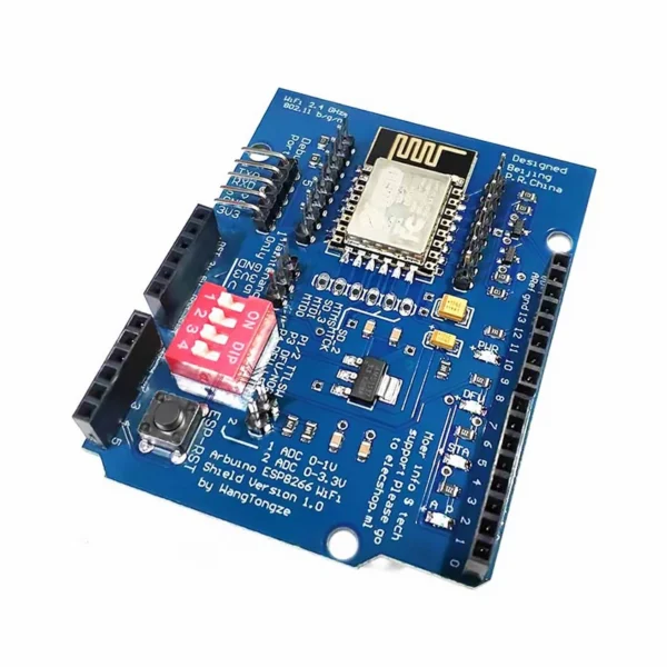 ESP8266 ESP-12E UART WIFI Wireless Shield Development Board For Arduino UNO R3 Circuits Boards Modules ONE
$3.90
ESP8266 ESP-12E UART WIFI Wireless Shield Development Board For Arduino UNO R3 Circuits Boards Modules ONE
$3.90