The architecture of AI data centers is undergoing a violent structural shift. As silicon roadmaps push toward NVIDIA’s Rubin and Rubin Ultra platforms, the industry is colliding with the physical limits of traditional copper cabling and ABF (Ajinomoto Build-up Film) substrates. To sustain the exponential growth of 224Gbps PAM4 signaling and HBM4 bandwidth, hardware architects are pivoting to two revolutionary paradigms: Orthogonal Backplanes and CoWoP (Chip-on-Wafer-on-PCB).
For hardware OEMs, signal integrity engineers, and procurement directors, these are not just buzzwords—they represent a fundamental rewriting of the PCB manufacturing rulebook. The line between "semiconductor packaging" and "printed circuit board fabrication" is vanishing.
This deep-dive guide explores the real-world manufacturing pain points, DFM (Design for Manufacturing) nightmares, and material realities of Orthogonal Backplanes and CoWoP, and why partnering with a specialized, high-layer-count PCB manufacturer is the only way to survive the AI hardware bottleneck.
The New AI Interconnect Paradigm
- What is an Orthogonal Backplane? A high-end switch architecture where line cards and switch fabric cards intersect vertically at a 90-degree angle. This eliminates long, lossy copper cables and traditional midplanes, drastically reducing signal insertion loss for 224G/448G networking.
- What is CoWoP? Chip-on-Wafer-on-PCB is an advanced packaging innovation that bypasses traditional IC substrates, mounting the silicon interposer directly onto a specialized, semiconductor-grade PCB platform.
- Why are they critical for 2026? They solve the twin bottlenecks of AI clusters: signal degradation over distance (solved by Orthogonal Backplanes) and ABF substrate capacity shortages (solved by CoWoP).
- The Manufacturing Reality: Both technologies require PCBs to perform like IC substrates, demanding 70+ layer counts, M9-grade ultra-low loss materials, and sub-micron registration tolerances.
Part 1: The Orthogonal Backplane – Eliminating the Midplane Bottleneck
In traditional high-end core routers and AI switches, signals travel from the line card, through a connector, across a massive midplane PCB, and into the switch fabric card. At 112Gbps, this was manageable. At 224Gbps and 448Gbps, the midplane acts as a massive low-pass filter, destroying signal integrity. Furthermore, thick midplanes choke airflow, creating thermal nightmares for 120kW AI racks.
The Orthogonal Solution: By crossing the line cards and fabric cards at a 90-degree angle, they connect directly via high-speed orthogonal connectors. The midplane is eliminated. The signal path is shortened to mere inches.
The DFM Nightmare: Manufacturing the 78-Layer Leviathan
While the architecture is elegant, manufacturing an Orthogonal Backplane is one of the most grueling challenges in modern electronics. Industry roadmaps for next-gen switch trees point toward massive, 78-layer M9-grade orthogonal backplanes.
Here is where standard PCB fabricators fail:
- Extreme Layer Count & Lamination Warpage: Pressing 70+ layers of ultra-low loss prepreg (like Panasonic Megtron 8 or M9 equivalents) requires multiple lamination cycles. The Z-axis Coefficient of Thermal Expansion (CTE) mismatch between the massive copper power planes and the resin system causes severe warpage. If the board warps more than a fraction of a percent, the orthogonal connectors will not seat, and automated SMT reflow will result in open circuits.
- Quartz Fabric Integration: To minimize the dielectric constant (Dk) and phase skew at 224G, engineers are specifying Quartz fabric (Q-Fabric) instead of traditional E-glass. Quartz is notoriously difficult to drill and desmear; it requires specialized laser parameters and chemical treatments to ensure reliable copper plating in high-aspect-ratio vias.
- Back-Drilling Precision: To prevent stub resonance at 112GHz Nyquist frequencies, thousands of plated through-holes (PTHs) must be back-drilled. The depth tolerance must be held within ±1 mil. A slight drill bit deflection in a 0.25-inch thick, 78-layer board will either leave a signal-destroying stub or drill into an active high-speed layer, scrapping a $20,000 board.
Part 2: CoWoP – When the PCB Becomes the Substrate
For the past three years, the AI industry has been held hostage by the ABF substrate shortage. TSMC’s CoWoS (Chip-on-Wafer-on-Substrate) relies on complex build-up substrates to connect GPU dies to HBM (High Bandwidth Memory). As AI chips grow to reticle-limit sizes, substrate capacity is maxed out.
Enter CoWoP (Chip-on-Wafer-on-PCB). CoWoP allows the industry to move closer to a vision of fully "package-less" systems by integrating the interposer directly onto a high-density PCB platform.
The Engineering Shift: PCB Fabrication Meets Semiconductor Packaging
In a CoWoP architecture, the PCB is no longer just a board; it is the foundational package substrate. This demands a manufacturing paradigm shift that 95% of traditional PCB houses cannot support.
- Ultra-Fine Line and Space (L/S): Standard AI server PCBs operate at 3mil/3mil L/S. CoWoP platforms require sub-5um to 10um L/S routing using Modified Semi-Additive Process (mSAP) or embedded die technologies to match the I/O density of the silicon interposer.
- Surface Roughness & Planarity: The PCB surface must be perfectly planar to accept the wafer-level bumping or micro-bumps of the interposer. Any resin starvation, glass protrusion, or copper roughness will cause micro-cracks during the thermal cycling of the AI cluster.
- Thermal Dissipation at the Core: CoWoP structures trap immense heat at the die-to-PCB interface. The PCB must integrate embedded copper coins, micro-via thermal arrays, and high-Tg materials to pull heat away from the logic die directly into the liquid cooling cold plates.
The Yield Crisis: Why Your Prototypes are Failing
Hardware startups and Tier-1 OEMs frequently report that their Orthogonal Backplane and CoWoP designs pass electromagnetic simulation (using tools like Ansys HFSS or Keysight ADS) but fail catastrophically on the manufacturing floor.
The Root Causes of Yield Loss:
- Glass Weave Skew: At 224G, routing traces over the "knuckles" of the fiberglass weave causes massive common-mode conversion. Manufacturers must utilize spread glass and enforce strict 10-degree routing angles, but maintaining registration across 70 layers of spread glass is a monumental optical inspection challenge.
- HVLP4 Copper Delamination: To minimize conductor loss, both Orthogonal and CoWoP designs mandate Hyper-Very-Low-Profile (HVLP4) copper foils. Because HVLP4 is essentially mirror-smooth, it lacks mechanical adhesion. If a fabricator uses legacy desmear chemistry, the inner layers will delaminate during the 260°C lead-free SMT reflow process.
- Impedance Discontinuities: The transition from the CoWoP interposer to the PCB micro-via, and eventually to the orthogonal connector, creates multiple impedance mismatches. Without advanced 3D X-ray and Time Domain Reflectometry (TDR) testing at the bare-board level, these discontinuities remain hidden until the system fails link training.
Strategic Sourcing: Securing Capacity in a Constrained Market
The transition to Orthogonal Backplanes and CoWoP is not just a technical challenge; it is a supply chain crisis. The exotic materials required—M9 laminates, Quartz fabric, HVLP4 foils, and specialized dry films—are heavily allocated. Lead times for these materials routinely exceed 20 to 24 weeks, and minimum order quantities (MOQs) are prohibitive for individual OEMs.
Furthermore, NVIDIA and other hyperscalers are quietly narrowing their CoWoP PCB partners to a select few capable of handling the semiconductor-grade tolerances. Attempting to source these materials and manage fabrication through fragmented, tier-2 vendors guarantees delayed time-to-market and compromised yield.
The ODM/OEM Advantage
To navigate this bottleneck, enterprise hardware teams must leverage strategic manufacturing partnerships. By initiating a consolidated ODM/OEM Bulk Inquiry, enterprise clients can bypass the open-market material shortages. A specialized manufacturing partner aggregates demand, securing priority allocations for M9 and Quartz materials, locking in pricing, and ensuring that the fabrication facility utilizes autoclaves and laser-drilling arrays specifically calibrated for CoWoP and 78-layer backplane tolerances.
Bridging the Gap: From Prototyping to Turnkey Volume
Developing an Orthogonal Backplane or a CoWoP test vehicle requires rapid iteration. You cannot afford to wait 12 weeks to discover that your via stub back-drilling depth was off by 2 mils.
Hardware teams require a partner capable of rapid-turnaround, high-complexity prototyping that scales seamlessly into volume production. This is where comprehensive Turnkey PCB Assembly and Manufacturing Services become your critical path to market.
A true turnkey partner doesn't just fabricate the bare board; they manage the entire ecosystem:
- Sourcing the unsourceable: Procuring exotic M8.5/M9 laminates and orthogonal connectors.
- Advanced DFM Feedback: Analyzing your stack-up for Z-axis CTE warpage and suggesting HDI micro-via staggering before the CAM tooling is cut.
- Precision SMT & Underfill: Handling the massive BGA footprints and specialized capillary underfill processes required for CoWoP interposers.
- Rigorous Validation: Performing 3D X-ray, flying probe, and high-frequency TDR testing to guarantee channel compliance before a single AI accelerator is socketed.
Advanced AI PCB Architectures
Q: What is the main advantage of an Orthogonal Backplane in AI switches?
A: An Orthogonal Backplane allows line cards and switch fabric cards to connect directly at a 90-degree angle, eliminating the need for a traditional midplane or long copper cables. This drastically reduces signal insertion loss and phase skew, which is mandatory for 224Gbps and 448Gbps PAM4 signaling in AI clusters verticalmind.
Q: How does CoWoP solve the ABF substrate shortage?
A: CoWoP (Chip-on-Wafer-on-PCB) bypasses the traditional ABF IC substrate entirely. By mounting the silicon interposer directly onto a specialized, ultra-high-density PCB platform, it relieves the bottleneck at semiconductor packaging houses and shifts the interconnect burden to advanced PCB manufacturers.
Q: What materials are required for 78-layer Orthogonal Backplanes?
A: Next-generation Orthogonal Backplanes require Extreme Low Loss (ELL) materials such as M9-grade laminates, often combined with Quartz (Q-Fabric) to minimize dielectric constant and glass weave skew, alongside HVLP4 copper foils to reduce conductor loss at high frequencies [[14], [15]].
Q: Why do CoWoP PCBs require sub-5um line and space routing?
A: Because CoWoP connects high-density silicon interposers directly to the PCB, the board must support I/O densities that rival traditional IC substrates. This requires Modified Semi-Additive Process (mSAP) manufacturing to achieve sub-5um to 10um line and space routing, which is beyond the capability of standard subtractive PCB etching
Engineering the Backbone of the AI Era
The era of treating the PCB as a passive, commoditized interconnect is over. As architectures like NVIDIA Rubin demand unprecedented bandwidth, Orthogonal Backplanes and CoWoP have emerged as the critical physical enablers of the AI revolution.
However, designing these systems is only half the battle. The manufacturing realities of 78-layer M9 laminates, Quartz fabric desmear, and semiconductor-grade CoWoP tolerances represent a massive barrier to entry. Hardware OEMs that attempt to force legacy manufacturing processes onto next-generation architectures will face catastrophic yield loss and delayed deployments.
To win in the AI hardware space, you must align your engineering team with a manufacturing partner that operates at the intersection of PCB fabrication and semiconductor packaging.

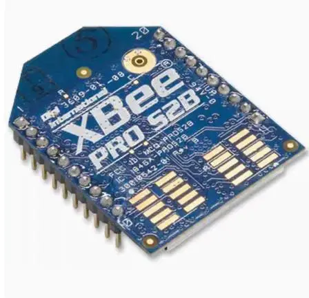 XBP24BZ7PIT-004 XBee-PRO ZB S2B module w/ PCB antenna
$51.90
XBP24BZ7PIT-004 XBee-PRO ZB S2B module w/ PCB antenna
$51.90
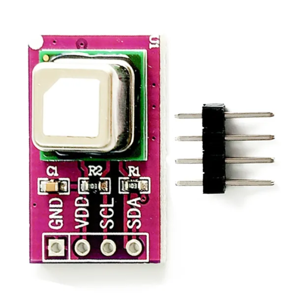 SCD40 SCD41 Gas Sensor Module I2C Communication 4PIN High Precision CO2 Temperature and Humidity 2 in 1 Detection Sensor
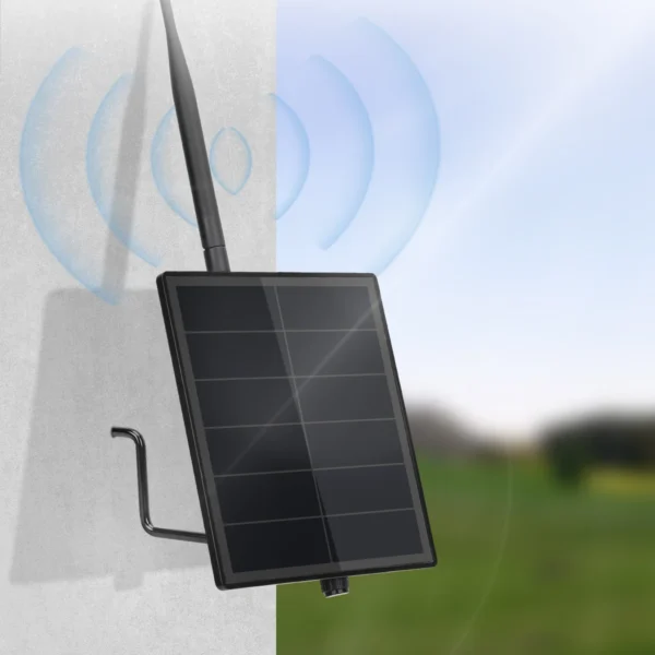 D5L H1 Meshtastic Mesh LoRa Node Repeater 5W Solar Power Kit 3.7v Output for Built in Heltec ESP32 V3 Lora Moudule IoT Device
$93.90
D5L H1 Meshtastic Mesh LoRa Node Repeater 5W Solar Power Kit 3.7v Output for Built in Heltec ESP32 V3 Lora Moudule IoT Device
$93.90
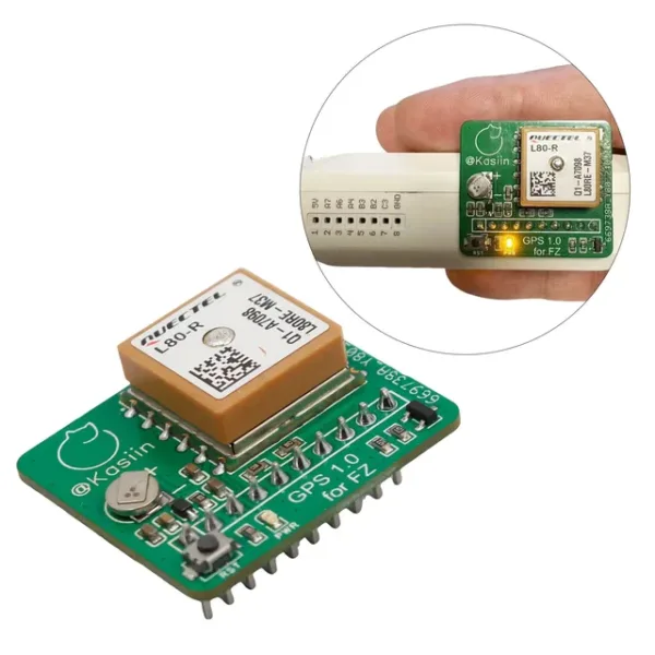 Flipper Zero WiFi Development Board, NRF24 + ESP32/NRF24 Multi-Board WiFi Development Board, GPS Module
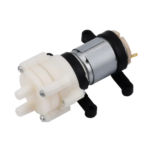 R385 Water Pump 12V Diaphragm Pump Pump 6V Small Miniature Water Pump Household Fish Tank Accessories Tea Set Water Pump
$2.30
R385 Water Pump 12V Diaphragm Pump Pump 6V Small Miniature Water Pump Household Fish Tank Accessories Tea Set Water Pump
$2.30