The announcement of the NVIDIA Rubin architecture has sent shockwaves through the hardware engineering community. Promising unprecedented leaps in AI training and inference via NVLink 6, HBM4, and next-generation SerDes, Rubin represents a paradigm shift in data center infrastructure. But for PCB designers and hardware architects, this leap in silicon performance introduces a brutal reality check: the interconnect is now the primary bottleneck.
As data rates push aggressively toward 224Gbps PAM4 and prepare for 448Gbps, legacy Ultra-Low Loss materials (like standard Megtron 7 or early Megtron 8) are hitting their physical limits. To maintain signal integrity (SI) and channel compliance in Rubin-based AI clusters, the industry is pivoting to M8.5+ and M9 Extreme Low Loss (ELL) laminates.
This guide dives deep into the manufacturing realities, DFM (Design for Manufacturing) nightmares, and supply chain strategies required to successfully prototype and mass-produce PCBs for the NVIDIA Rubin platform.
The Shift to M8.5+ and M9
- What is NVIDIA Rubin? NVIDIA's next-generation AI architecture (post-Blackwell) requiring massive bandwidth, targeting NVLink 6 and PCIe Gen 7 preparation.
- What are M8.5+ and M9 Materials? Next-generation Extreme Low Loss (ELL) PCB laminates engineered specifically to minimize insertion loss and phase skew at 224Gbps and 448Gbps data rates.
- Why are they needed? At 224G PAM4, dielectric losses and copper surface roughness cause catastrophic signal degradation. M9 materials offer a significantly lower Dissipation Factor (Df) and utilize ultra-smooth HVLP4 copper foils.
- The Core Manufacturing Pain Point: M8.5/M9 resins are highly brittle and require specialized lamination and desmear processes to prevent delamination and via-barrel cracking during thermal cycling.
The Signal Integrity Crisis: Why M8 is No Longer Enough for Rubin
To understand the necessity of M8.5+ and M9 materials, we must look at the physics of 224Gbps PAM4 signaling. At these frequencies, the Nyquist frequency is 112 GHz. The signal channel is essentially acting as a massive low-pass filter.
In current Blackwell-era designs utilizing Megtron 8 (M8), designers are already maxing out their loss budgets. When you factor in connector losses, via stubs, and BGA escape routing, the PCB trace itself must be virtually lossless.
M8 vs. M8.5+ / M9: The Material Breakdown
The Engineer's Pain Point: If you simulate your 224G Rubin baseboard using standard M8 parameters, your channel might pass in simulation. However, once manufactured, the real-world insertion loss and return loss will likely fail compliance. M9 materials utilize advanced hydrocarbon and PTFE-based resin systems that dramatically flatten the loss curve across the 50GHz–100GHz spectrum, providing the necessary margin for Rubin’s aggressive equalization (EQ) requirements.
The Manufacturing Nightmare: DFM Challenges with ELL Materials
Here is where the gap between SI simulation and factory reality widens. As a specialized PCB manufacturer, we see hardware teams struggle with yield rates when transitioning to M8.5+ and M9 materials. These Extreme Low Loss laminates are notoriously difficult to fabricate.
1. The Desmear and HVLP Peel Strength Dilemma
To achieve the ultra-low conductor loss required for 224G, M9 materials mandate the use of HVLP4 (Hyper Very Low Profile) or near-profile-free copper foils. The surface roughness (Rz) is practically zero.
- The Problem: Smooth copper means terrible mechanical adhesion (peel strength).
- The Factory Solution: Fabricators must use highly aggressive, specialized chemical desmear processes and alternative black-oxide/alternative micro-etching treatments to "bite" into the HVLP4 foil without destroying its smooth electrical surface. If a standard FR-4 desmear process is used on M9 material, the inner layers will delaminate during the SMT reflow process.
2. Z-Axis CTE and Microvia Reliability
M8.5+ and M9 resin systems have different Coefficient of Thermal Expansion (CTE) profiles compared to standard epoxies. When a 30+ layer AI server board goes through the 260°C lead-free reflow process, the Z-axis expansion can tear the copper plating inside high-aspect-ratio microvias.
- The DFM Fix: Designers must work with their Turnkey PCB Assembly Manufacturing partner early to optimize the via stack-up. Utilizing staggered microvias, filled vias, and capped vias (Any-Layer HDI) is mandatory to prevent barrel cracking and ensure the long-term reliability of Rubin GPU baseboards.
3. Glass Weave Skew and Spread Glass
At 112G and 224G, the Glass Weave Skew effect is fatal. Standard E-glass bundles have a different dielectric constant (Dk ≈ 6.5) than the surrounding resin (Dk ≈ 3.0). If a differential pair routes through a glass bundle on one trace and through resin on the other, it creates massive phase skew (common-mode conversion), destroying the signal.
- The Material Requirement: M8.5+ and M9 stack-ups strictly require Spread Glass (mechanically flattened glass cloth) or specialized low-Dk NE-glass to homogenize the dielectric environment. This drastically increases material costs and requires precise routing angles (e.g., 10-degree routing) by the layout team.
Strategic Sourcing: Navigating the M9 Supply Chain Bottleneck
For Procurement Managers and Supply Chain Directors, the technical superiority of M9 materials comes with a severe logistical headache.
Because the formulation of M9 and advanced M8.5+ laminates relies on specialized resins and ultra-low-profile copper foils (which are heavily allocated to top-tier AI networking and aerospace clients), lead times currently stretch from 16 to 24 weeks. Furthermore, the minimum order quantities (MOQs) for these exotic prepregs are massive.
Attempting to source M9 laminates and manage the fabrication of a 40-layer Rubin switch board through fragmented vendors is a recipe for delayed time-to-market. Hardware OEMs are increasingly relying on strategic manufacturing partnerships to secure material allocations.
By initiating a consolidated ODM/OEM Bulk Inquiry, enterprise clients can leverage a manufacturer's aggregate purchasing power. This ensures priority access to Panasonic, Isola, or AGC’s latest Extreme Low Loss laminates, locks in pricing against volatile copper and resin markets, and guarantees that the fabrication house has the specific autoclaves and lamination presses calibrated for M9's unique thermal profiles.
Bridging Prototyping and Mass Production for AI Hardware
The transition from a Rubin simulation to a functional AI server cluster requires a phased approach to manufacturing.
- Phase 1: SI Validation & Prototyping. You need a partner capable of rapid-turnaround turnkey PCBA to test your M8.5 channel designs, validate TDR impedance, and perform 3D X-ray inspections on microvia fill quality. Rapid prototyping services allow you to iterate your spread-glass routing and via stub back-drilling depths before committing to mass production.
- Phase 2: DFM & Yield Optimization. Before scaling, your manufacturing partner must conduct rigorous Design for Manufacturing reviews, identifying potential warpage issues caused by asymmetric copper distribution across 40+ layers of M9 material.
- Phase 3: Volume ODM/OEM Production. Scaling to thousands of AI baseboards requires automated optical inspection (AOI) tailored to HVLP4 traces, automated X-ray for BGA pad integrity, and robust functional testing under thermal loads.
For hardware teams building the next generation of AI infrastructure, your choice of manufacturing partner is just as critical as your choice of silicon.
NVIDIA Rubin & M9 PCB Materials
Q: What data rates do M8.5+ and M9 PCB materials support?
A: M8.5+ materials are optimized for reliable 112Gbps to 224Gbps PAM4 signaling, while M9 (Extreme Low Loss) materials are specifically engineered to support 224Gbps and future 448Gbps data rates required by architectures like NVIDIA Rubin and PCIe Gen 7.
Q: What is the main manufacturing risk when using M9 PCB laminates?
A: The primary risk is delamination due to poor peel strength. M9 materials require ultra-smooth HVLP4 copper foils to minimize signal loss. Fabricators must use highly specialized chemical desmear and micro-etching processes to ensure adhesion without ruining the foil's electrical smoothness.
Q: How does Glass Weave Skew affect 224G PCB routing?
A: At 224Gbps, the difference in dielectric constant between fiberglass bundles and resin causes severe phase skew (timing mismatch) between differential pairs. Designers must use "Spread Glass" materials and route traces at specific angles (e.g., 10 to 15 degrees) to prevent signal degradation.
Q: How can OEMs secure M9 materials with such long lead times?
A: Due to high demand for AI hardware, M9 materials often have 16+ week lead times. OEMs should partner with specialized PCBA manufacturers who can aggregate demand, secure bulk allocations from laminate suppliers, and manage the entire supply chain through an ODM/OEM partnership.
Engineering the Backbone of AI
The NVIDIA Rubin platform will define the next era of artificial intelligence, but its success relies entirely on the physical interconnects that power it. M8.5+ and M9 Extreme Low Loss materials are not just incremental upgrades; they are fundamental requirements to overcome the physics of 224Gbps signaling.
However, specifying the right material is only the first step. Overcoming the DFM challenges of HVLP copper, mitigating glass weave skew, and securing a reliable supply chain requires deep manufacturing expertise. Do not let PCB fabrication bottlenecks derail your AI hardware roadmap.

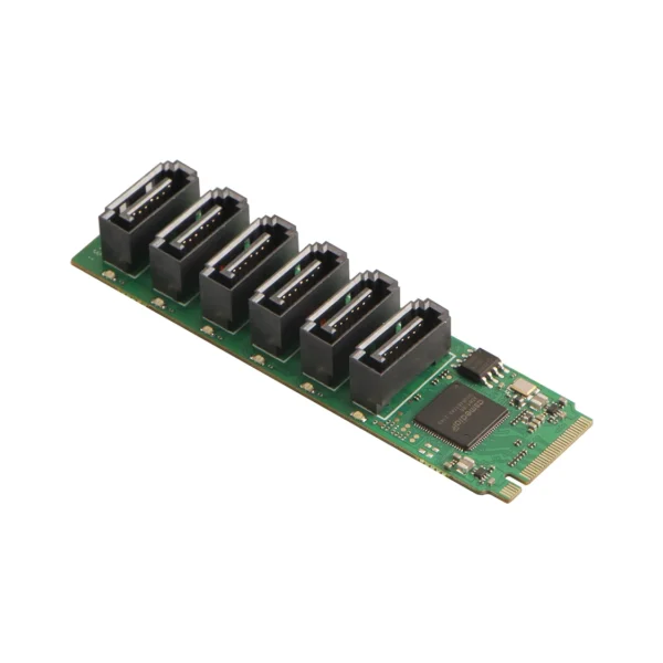 Radxa M.2 to 6x SATA Adapter, M.2 M Key Interface, 6x SATA 3.0 Ports
$32.50
Radxa M.2 to 6x SATA Adapter, M.2 M Key Interface, 6x SATA 3.0 Ports
$32.50
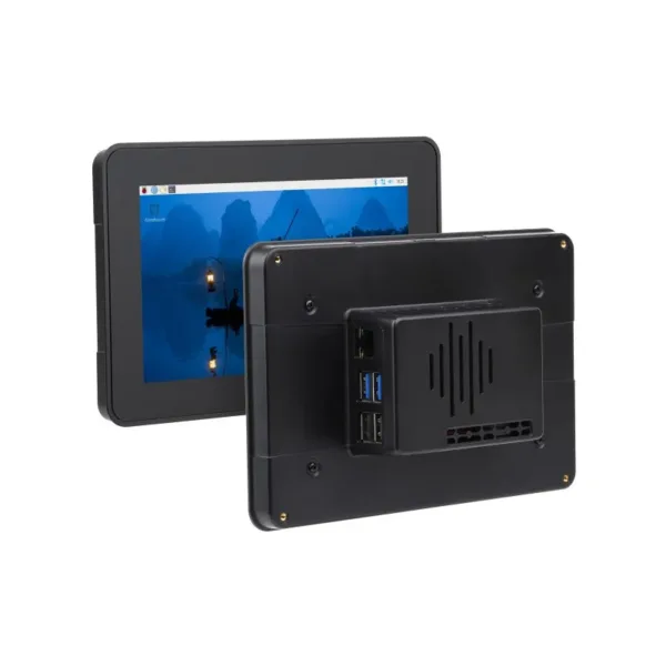 Protective Case for Raspberry Pi 7 Inch Touch Display 2 And Raspberry Pi 5 Compatible with Multiple 7 Inch Screens
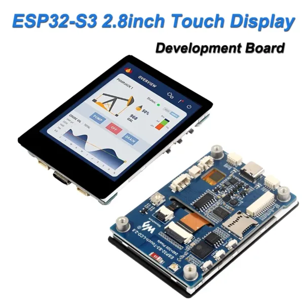 ESP32-S3 2.8 inch IPS Touchscreen Development Board 5-point 240x320 Touch Display Support WiFi Bluetooth HMI/LVGL GUI
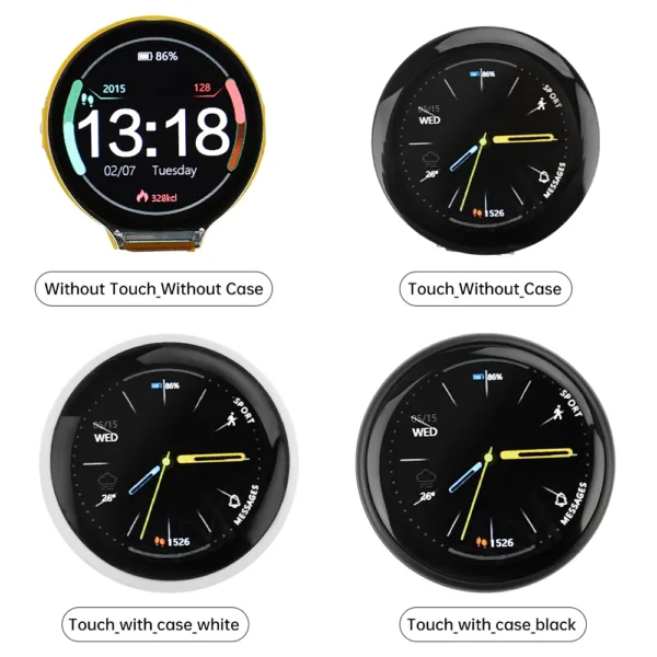 ESP32-C3-MINI-1U Development Board 1.28 Inch 240*240 IPS Smart Display Screen LCD TFT Module WiFi & Bluetooth With Touch
 HT16K33 LED Display Module for Arduino 4 Digit 7 Segment 0.56 inch Time Clock Indicator Tube Module Red Blue Green Yellow White
$4.90
HT16K33 LED Display Module for Arduino 4 Digit 7 Segment 0.56 inch Time Clock Indicator Tube Module Red Blue Green Yellow White
$4.90