Why PCB Thickness is a Critical Engineering Parameter
In the electronics manufacturing ecosystem, many designers blindly accept the default "1.6mm" thickness in their CAD software without a second thought. While 1.6mm (0.062") is indeed the most common standard PCB thickness, treating it as a universal constant is a critical engineering oversight.
The thickness of a printed circuit board is not merely a physical dimension; it is a foundational variable that influences:
- Signal Integrity: The distance between signal layers and reference planes dictates the dielectric spacing required for controlled impedance (e.g., 50Ω single-ended or 100Ω differential).
- Mechanical Rigidity: The board must support heavy components (like large transformers or connectors) without flexing, which can crack solder joints.
- Thermal Management: Thicker copper and substrate materials provide greater thermal mass and heat dissipation pathways.
- Form Factor Constraints: Wearables demand ultra-thin boards (0.4mm - 0.8mm), while industrial backplanes require thick, robust boards (2.4mm - 3.2mm).
Understanding how to select and specify the correct PCB thickness is a mandatory discipline for any hardware team aiming to avoid costly respins and ensure high-yield manufacturing.
Standard PCB Thickness by Layer Count: A Practical Guide
While 1.6mm is the overarching standard, the achievable and recommended thicknesses vary based on the number of copper layers. Below is a practical reference guide for standard rigid PCB thicknesses:
Expert Insight: The industry standard thickness tolerance is typically ±10%. For a 1.6mm board, this means the final thickness can legally range from 1.44mm to 1.76mm. If your design requires tighter tolerances (e.g., ±5%), this must be explicitly specified during the quoting process, as it may impact cost and manufacturing yield.
Top 3 PCB Thickness Manufacturing Pain Points (And How We Solve Them)
As a hardware developer or supply chain manager, your goal is a high first-pass yield. Incorrect thickness specification is a leading cause of assembly and reliability failures. Here is how a professional manufacturing partner mitigates these risks:
1. Edge Connector Mating Failures (The "Gold Finger" Problem)
The Pain Point: Boards that plug directly into a motherboard or backplane (e.g., PCIe cards, memory modules, or custom edge connectors) require strict thickness control. If the PCB is too thick (e.g., 1.7mm), it will not fit into the connector slot. If it is too thin (e.g., 1.5mm), the connector pins will not make sufficient contact pressure, leading to intermittent signal loss.
Our Solution: For edge-connector applications, we enforce a strict ±5% thickness tolerance (e.g., 1.6mm ±0.08mm). We also utilize specialized routing and chamfering processes to ensure the "gold fingers" are perfectly beveled, preventing damage to the mating connector during insertion.
2. Via Aspect Ratio Limitations in Thick Boards
The Pain Point: The "Aspect Ratio" is the ratio of the PCB thickness to the diameter of the drilled hole. For example, a 3.2mm thick board with a 0.3mm drilled via has an aspect ratio of 10:1. High aspect ratios make it incredibly difficult for electroplating solutions to penetrate the hole, leading to "voids" or incomplete copper plating inside the via, which causes open circuits.
Our Solution: Our CAM (Computer-Aided Manufacturing) engineers automatically calculate the aspect ratio of your design. If it exceeds standard manufacturing capabilities (typically >8:1 for standard through-holes, or >10:1 for advanced facilities), we will proactively recommend increasing the via diameter or utilizing advanced techniques like via-in-pad or staggered microvias to ensure 100% reliable plating.
3. Warpage and Bow/Twist in Thin or Asymmetric Boards
The Pain Point: Using a thin substrate (e.g., 0.8mm) for a 4-layer board with heavy copper (2oz or 3oz) on one side and light copper (0.5oz) on the other creates asymmetric thermal stress. During the high heat of SMT reflow soldering, the board will warp, twist, or bow. This leads to misaligned components, solder bridging, and "open" joints.
Our Solution: We perform rigorous stack-up symmetry analysis during the DFM review. If a thin, heavy-copper design is required, we balance the copper distribution by adding "thieving" (dummy copper patterns) to the lighter layers. We also customize the lamination and reflow thermal profiles to minimize thermal shock and guarantee a flat, stable board.
The Ultimate DFM Checklist for PCB Thickness
To ensure your design is 100% manufacturable and reliable, your layout must adhere to these industry-proven DFM rules regarding board thickness:
- Match Thickness to Connector Specs: If your board uses a card-edge connector, verify the connector datasheet. Most require 1.6mm ±0.1mm. Do not deviate without consulting the manufacturer.
- Recalculate Impedance for Non-Standard Thicknesses: If you change the overall board thickness from 1.6mm to 1.2mm, the dielectric spacing between your signal layer and ground plane changes. You must work with your manufacturer to recalculate and adjust your trace widths to maintain your target impedance (e.g., 50Ω).
- Respect the Aspect Ratio: Keep the via aspect ratio (Board Thickness ÷ Finished Hole Diameter) below 8:1 for standard through-hole vias to guarantee reliable copper plating.
- Balance Copper Distribution: For boards thinner than 1.0mm, ensure that the copper weight and distribution are as symmetrical as possible across the layer stack to prevent warpage.
- Consider the Final Enclosure: Verify that the chosen PCB thickness, combined with the height of the tallest components and the solder fillets, will physically fit inside your product’s mechanical enclosure.
Why Partner with a Professional PCB Thickness & Assembly Manufacturer?
Specifying the right PCB thickness is only half the battle; manufacturing it to precise tolerances and assembling it without defects requires advanced capabilities. Sourcing bare boards from one vendor and assembly from another often leads to finger-pointing when warpage or impedance issues occur.
You need a unified, accountable partner who controls the entire process. We bridge the gap between theoretical design and high-yield manufacturing reality:
- Proactive DFM & Stack-up Engineering: Before production begins, our engineering team reviews your Gerber files and layer stack-up. We verify thickness tolerances, via aspect ratios, and copper balance, providing you with a detailed, free DFM report to eliminate mechanical and electrical risks before any materials are cut.
- Seamless Prototyping to Turnkey Assembly: Whether you are building a space-constrained wearable device requiring a 0.8mm 4-layer board, or a robust industrial controller needing a 2.4mm heavy-copper board, our turnkey PCB assembly manufacturing service handles the entire lifecycle. We manage the BOM, source authentic components, and utilize precision SMT processes calibrated to your board’s specific thermal mass and thickness. Discover how we simplify your workflow: PCB Prototype & Turnkey PCB Assembly Manufacturing.
- Scalable OEM/ODM Bulk Production: When your design is validated, scaling to mass production requires unwavering consistency. We utilize automated thickness gauging, 3D Automated Optical Inspection (AOI), and strict IPC-6012 Class 2/3 standards to guarantee that every single unit meets your exact mechanical and electrical specifications. Request a detailed, competitive quote for your next large-scale project: OEM/ODM Bulk Inquiry.
Frequently Asked Questions (FAQ)
Q1: Can I order a custom PCB thickness that is not listed in your standard options?
A: Yes. While we maintain large inventories of standard thicknesses (like 1.6mm) for fast turnaround, we can custom-build stack-ups to achieve almost any thickness (e.g., 1.3mm, 1.8mm, 2.5mm) by combining specific core and prepreg layers. Note that highly non-standard thicknesses may have slightly longer lead times and higher costs due to material sourcing.
Q2: How does PCB thickness affect impedance control?
A: Impedance is directly proportional to the distance between the signal trace and its reference plane (dielectric thickness). If you make a board thinner, the dielectric layer becomes thinner. To maintain the same impedance (e.g., 50Ω), the trace width must be narrowed. Our engineering team will recalculate this for you during the DFM review.
Q3: What is the thinnest PCB thickness you can manufacture?
A: For rigid FR-4 PCBs, we can reliably manufacture down to 0.4mm for 1- or 2-layer boards. For multilayer boards, 0.8mm is typically the practical minimum to maintain structural integrity and prevent severe warpage during assembly. For extreme flexibility, we recommend transitioning to Flexible PCBs (FPC) using Polyimide.
Q4: Does a thicker PCB cost more to manufacture?
A: Not necessarily. A standard 1.6mm board is often the most cost-effective because it uses standard, high-volume materials. However, extremely thick boards (e.g., 3.2mm+) can cost more due to the specialized, heavy-duty drilling equipment required and the increased amount of raw material used.
Precision Thickness is the Foundation of Reliability
The thickness of your PCB is far more than a simple CAD parameter; it is a critical determinant of your product’s mechanical survival, signal integrity, and assembly yield. Blindly accepting default values or deviating from standards without proper DFM analysis is a direct invitation to costly field failures and manufacturing delays.
By understanding the engineering implications of PCB thickness and partnering with a manufacturer that possesses the specialized equipment and expertise to hold tight tolerances, you transform a potential vulnerability into a robust, scalable advantage.

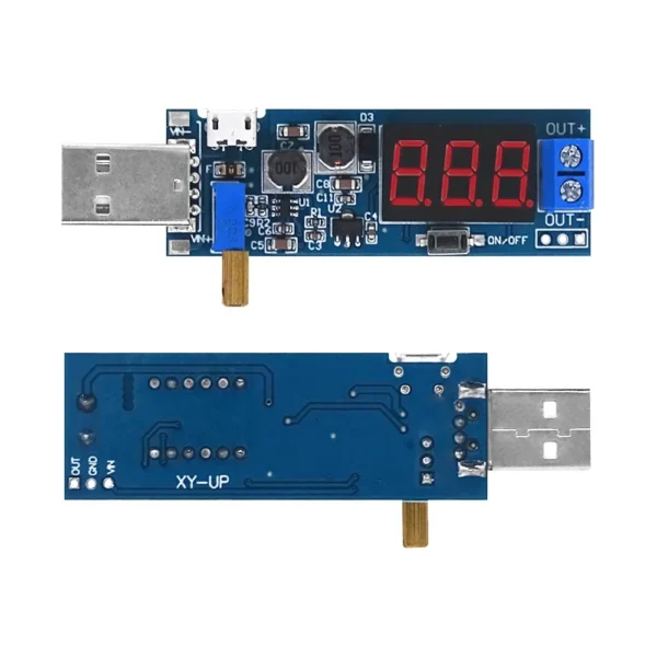 DC-DC USB step-up/step-down power supply voltage regulator module 5V to 3.3V 9V 12V 24V converter output DC 1.2V-24V
$3.90
DC-DC USB step-up/step-down power supply voltage regulator module 5V to 3.3V 9V 12V 24V converter output DC 1.2V-24V
$3.90
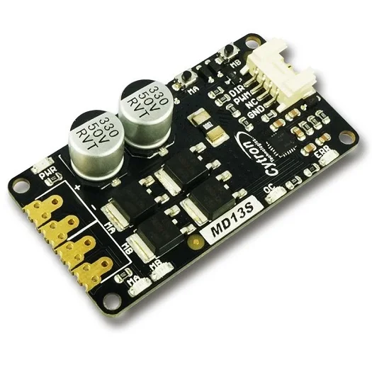 MD13S-Cytron 13Amp Motor Driver development board 108070021
$26.90
MD13S-Cytron 13Amp Motor Driver development board 108070021
$26.90
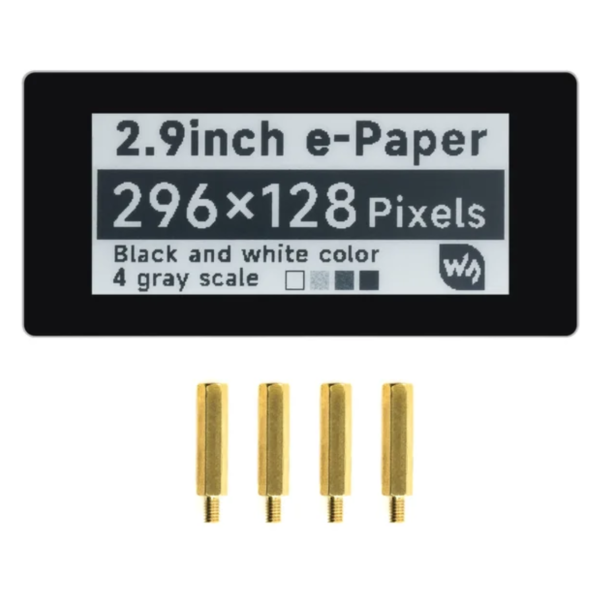 2.9inch Touch E-Paper Module, Capacitive Touch, Partial Refresh, Low Power, Wide Viewing Angle, Paper-like Effect
$23.90
2.9inch Touch E-Paper Module, Capacitive Touch, Partial Refresh, Low Power, Wide Viewing Angle, Paper-like Effect
$23.90
 A33T-ESP32 S3 2.1 Inch Round Rotary LCD Touch Knob Display Development Bluetooth Wifi LVGL Black
$35.90
A33T-ESP32 S3 2.1 Inch Round Rotary LCD Touch Knob Display Development Bluetooth Wifi LVGL Black
$35.90
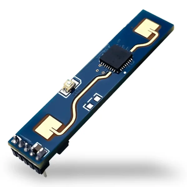 Human Presence Sensor Module 24GHz Smart Millimeter Wave Radar Sensing Heartbeat Detection Module with BT HLK-LD2410B
$4.90 – $5.90Price range: $4.90 through $5.90
Human Presence Sensor Module 24GHz Smart Millimeter Wave Radar Sensing Heartbeat Detection Module with BT HLK-LD2410B
$4.90 – $5.90Price range: $4.90 through $5.90