Why Package Selection Dictates PCB Reliability
In modern electronics design, the choice between QFN and QFP is rarely just about pin count; it is a fundamental decision that impacts the entire product lifecycle. As devices shrink and performance demands rise (e.g., 5G IoT modules, automotive sensors, and wearable tech), the industry has aggressively shifted toward QFN and similar bottom-termination packages.
However, this miniaturization comes at a cost. The margin for error in SMT (Surface Mount Technology) assembly shrinks dramatically. A poorly designed QFN footprint or an incorrect reflow profile can result in catastrophic, hidden defects like thermal pad voiding or intermittent open circuits. Conversely, forcing a high-pin-count QFP into a dense design can lead to routing nightmares and fragile leads that fail under mechanical vibration.
Understanding the manufacturing realities of both packages is a mandatory discipline for any hardware team aiming to achieve high first-pass yields and long-term field reliability.
Deep Dive: QFN (Quad Flat No-leads) Packaging
What it is: A QFN package features flat, metallic terminations along the bottom perimeter of the package, with no leads extending outward. Crucially, most QFNs include a large, exposed metal pad (EPAD) in the center of the bottom surface.
The Engineering Advantages
- Superior Thermal Management: The central EPAD provides a direct, low-resistance thermal path from the silicon die to the PCB’s ground plane or dedicated thermal vias. This can reduce thermal resistance (θJA) by up to 50% compared to a QFP.
- Enhanced Electrical Performance: The absence of long gull-wing leads drastically reduces parasitic inductance and capacitance. This is critical for high-frequency RF, high-speed digital, and power management ICs.
- Minimal Footprint: QFNs occupy significantly less board area, enabling ultra-compact designs.
The Manufacturing Pain Points
- Solder Voiding: The large EPAD traps flux volatiles during reflow, leading to air pockets (voids) in the solder joint. Excessive voiding (>25% per IPC Class 3) compromises thermal transfer and mechanical strength.
- Hidden Joints: Because the solder joints are underneath the package, standard top-down Automated Optical Inspection (AOI) cannot verify solder quality.
- Solder Starvation: Capillary action can pull too much solder paste down into the thermal vias (if not properly plugged), leaving insufficient solder for the perimeter pads.
Deep Dive: QFP (Quad Flat Package) Packaging
What it is: A QFP package features thin, flat, "gull-wing" shaped leads that extend outward from all four sides of the package and are soldered to the PCB surface.
The Engineering Advantages
- Excellent Inspectability: All solder joints are visible on the outside of the package. AOI systems and human technicians can easily verify solder fillet formation, making quality control straightforward.
- Forgiving Assembly: The gull-wing lead provides a degree of mechanical compliance, absorbing minor Z-axis thermal expansion mismatches between the component and the PCB.
- Ease of Rework: QFP components can be relatively easily removed and replaced using standard hot-air rework stations, making them ideal for prototyping and low-volume production.
The Manufacturing Pain Points
- Solder Bridging: As pin pitches shrink (e.g., 0.4mm or 0.5mm), the risk of solder paste spreading and connecting adjacent leads during reflow increases dramatically.
- Lead Damage: The exposed gull-wing leads are fragile. They can be bent or damaged during shipping, tape-and-reel handling, or the pick-and-place process, leading to coplanarity issues and open circuits.
- Larger Footprint & Parasitics: The outward-extending leads consume valuable PCB real estate and introduce unwanted inductance, making QFP unsuitable for high-frequency applications.
QFN vs. QFP: A Technical Decision Matrix
When choosing between these packages, use this data-driven comparison to validate your design direction:
Top 3 SMT Assembly Pain Points (And How We Solve Them)
As a hardware developer or supply chain manager, your goal is to eliminate preventable yield loss. Here is how a professional manufacturing partner mitigates the most common QFN/QFP failures:
1. Eliminating QFN Solder Voiding
The Pain Point: Flux gases get trapped under the large, flat EPAD during reflow, creating voids that act as thermal insulators and weaken the mechanical bond.
Our Solution: We employ a multi-pronged approach to void reduction:
- Stencil Optimization: We do not use a 1:1 solid aperture for the thermal pad. Instead, we design a checkerboard, split, or cross-hatch aperture pattern. This allows flux gases to escape through the gaps while maintaining sufficient solder volume for thermal and mechanical connection.
- Solder Paste Selection: We recommend Type 4 or Type 5 solder paste for fine-pitch QFNs, which features smaller powder particles that flow more evenly and reduce voiding.
- Thermal Profiling: We customize the reflow profile with an extended, controlled "soak" zone to gently evaporate flux volatiles before the solder reaches its liquidus state.
2. Preventing QFP Solder Bridging and Lead Damage
The Pain Point: Excess solder paste or misalignment causes adjacent gull-wing leads to short together. Alternatively, bent leads prevent proper contact with the pad.
Our Solution: Our CAM engineers apply strict aperture reduction (typically 10-15% for fine-pitch QFPs) to the stencil design to prevent paste overflow. Furthermore, our pick-and-place machines are calibrated with precise placement force and post-placement vision inspection to ensure perfect lead-to-pad alignment before the board enters the reflow oven.
3. PCB Land Pattern (Footprint) Errors
The Pain Point: Designers often copy-paste footprints from unreliable online libraries. An incorrect pad size or missing thermal vias under a QFN will guarantee assembly failure, regardless of how good the assembly house is.
Our Solution: We provide a complimentary, rigorous DFM (Design for Manufacturability) review. We verify your land patterns against IPC-7351 standards, check thermal via placement (ensuring they are plugged or tented to prevent solder wicking), and validate solder mask clearances before any manufacturing begins.
The Ultimate DFM Checklist for QFN & QFP Assembly
To ensure your design is 100% manufacturable, verify your CAD layout against these industry-proven rules:
- QFN Thermal Via Management: If placing thermal vias under the QFN EPAD, they must be plugged (filled with non-conductive epoxy) and plated over, or at minimum, tented with solder mask on the bottom side. Unplugged vias will wick solder away from the joint, causing starvation.
- Stencil Aperture Reduction: For QFN perimeter pads, reduce the stencil aperture by 10-20% to prevent solder bridging. For the QFN EPAD, use a segmented (checkerboard) pattern covering 50-70% of the pad area.
- QFP Solder Mask Dams: Ensure a continuous solder mask dam exists between adjacent QFP pads to prevent solder from flowing laterally and causing bridges.
- Keep-Out Zones: Maintain a minimum 3mm keep-out zone around QFN packages to allow for X-ray inspection access and potential rework tool clearance.
- Copper Balance: Ensure symmetrical copper distribution around QFP pads to prevent the component from "tombstoning" or shifting due to uneven surface tension during reflow.
Why Partner with esp32s.com for QFN/QFP Assembly?
Choosing the right package is only half the battle; assembling it correctly requires advanced equipment, deep process expertise, and rigorous quality control. Sourcing bare boards from one vendor and SMT assembly from another often leads to finger-pointing when hidden defects like QFN voiding occur.
You need a unified, accountable partner. At esp32s.com, we bridge the gap between theoretical design and high-yield manufacturing reality:
- Proactive DFM & Footprint Validation: Before production begins, our engineering team reviews your Gerber and centroid files. We flag potential QFN thermal via wicking risks, QFP bridging hazards, and stencil design flaws, providing actionable solutions before any metal is cut.
- Advanced Inspection Capabilities: We do not guess about hidden solder joints. Our facility is equipped with high-resolution 3D X-Ray Inspection (AXI) systems specifically calibrated to measure QFN thermal pad voiding percentages and verify perimeter joint integrity, ensuring strict compliance with IPC-A-610 Class 2/3 standards.
- Seamless Prototyping to Turnkey Assembly: Whether you are prototyping a complex RF module with ultra-fine-pitch QFNs or scaling a consumer device with QFP microcontrollers, our turnkey PCB assembly manufacturing service handles the entire lifecycle. We manage the BOM, source authentic components, and execute precision SMT processes. Discover how we simplify your workflow: PCB Prototype & Turnkey PCB Assembly Manufacturing.
- Scalable OEM/ODM Bulk Production: When your design is validated, scaling to mass production requires unwavering consistency. We utilize closed-loop Solder Paste Inspection (SPI), customized reflow profiling, and strict process controls to guarantee high yield and competitive pricing for large-scale runs. Request a detailed quote for your next project: OEM/ODM Bulk Inquiry.
FAQ
Q1: Can QFN components be manually soldered or reworked?
A: Yes, but it is challenging and requires specialized tools. It typically involves a hot air rework station, a custom nozzle matching the QFN size, and high-activity flux. Due to the hidden joints, rework should always be followed by X-ray inspection to verify the new joint quality. For this reason, QFN is less ideal for hobbyist or low-tech manual assembly.
Q2: What is the acceptable percentage of solder voiding in a QFN thermal pad?
A: According to IPC-A-610 Class 2 (general commercial electronics), total voiding should not exceed 25% of the joint area. For Class 3 (high-reliability, automotive, medical, aerospace), the requirement is stricter, often demanding <15% or even <10% voiding. Our optimized stencil designs and reflow profiles are specifically tuned to meet these stringent requirements.
Q3: How do I prevent solder from wicking down thermal vias under a QFN?
A: The most reliable method is to specify Via-in-Pad Plated Over (VIPPO), where the vias are filled with non-conductive resin and flattened. A more cost-effective alternative is to ensure the vias are fully "tented" (covered) by solder mask on the bottom side of the PCB, which blocks the solder from flowing through during reflow.
Q4: Do you provide assembly services for mixed-technology boards (both QFN and QFP)?
A: Absolutely. Mixed-technology boards are very common. Our turnkey service seamlessly handles both. We optimize the stencil design to accommodate the fine-pitch requirements of the QFN while ensuring sufficient paste volume for the QFP gull-wing leads, all within a single, optimized reflow profile.
Precision Assembly is Non-Negotiable
The choice between QFN and QFP packaging fundamentally shapes your product’s thermal performance, electrical integrity, and physical footprint. While QFN offers undeniable advantages for modern, high-performance electronics, its hidden joints and susceptibility to voiding demand a higher level of manufacturing sophistication.
By adhering to strict IPC DFM guidelines and partnering with a manufacturer that possesses the advanced equipment (X-ray inspection, precision stenciling) and deep process expertise to handle these packages, you transform a high-risk assembly challenge into a reliable, scalable competitive advantage.

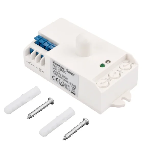 5.8G Microwave Radar Sensor Switch AC 220V/ DC12V-24V Intelligent Energy Saving Control Microwave Radar Sensor
$5.90 – $6.30Price range: $5.90 through $6.30
5.8G Microwave Radar Sensor Switch AC 220V/ DC12V-24V Intelligent Energy Saving Control Microwave Radar Sensor
$5.90 – $6.30Price range: $5.90 through $6.30
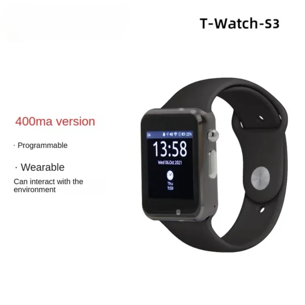 T-Watch-S3 ESP32-S3 Programmable LoRa WiFi Bluetooth PMU Touchable Watch
$52.90
T-Watch-S3 ESP32-S3 Programmable LoRa WiFi Bluetooth PMU Touchable Watch
$52.90
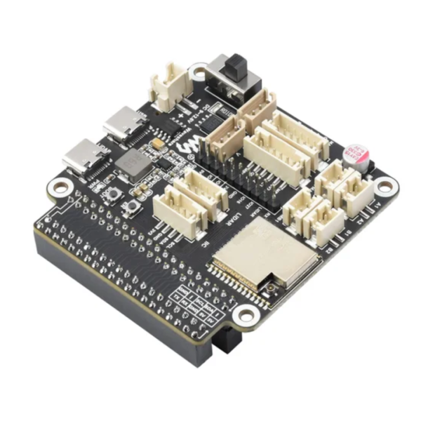 General Driver board for Robots, for Raspberry Pi and Jetson Nano, Supports WIFI, Bluetooth and ESP-NOW Communications
$32.90
General Driver board for Robots, for Raspberry Pi and Jetson Nano, Supports WIFI, Bluetooth and ESP-NOW Communications
$32.90
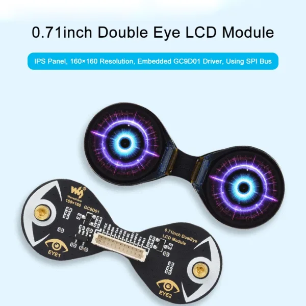 0.71inch Double Eye Round LCD Display Module Option SPI 160x160 65K Colors For Arduino Raspberry Pi ESP32 Pico STM32
 LMT70 module High precision medical temperature sensor LMT70YFQR temperature monitoring
$15.90
LMT70 module High precision medical temperature sensor LMT70YFQR temperature monitoring
$15.90