For the past three years, the AI and High-Performance Computing (HPC) industry has been held hostage by a single, critical bottleneck: Advanced Packaging Capacity. Specifically, TSMC’s CoWoS (Chip-on-Wafer-on-Substrate) and the global shortage of ABF (Ajinomoto Build-up Film) substrates have dictated the production timelines of the world’s most powerful AI accelerators and data center GPUs.
But a paradigm shift is underway. As hyperscalers and silicon architects push toward reticle-limit die sizes and 224G PAM4 interconnects, the traditional IC substrate is hitting its physical and economic limits. Enter CoWoP (Chip-on-Wafer-on-PCB / Chip-on-Wafer-on-Panel).
CoWoP represents a radical architectural pivot: eliminating the traditional IC substrate entirely and mounting the silicon interposer or wafer-level package directly onto a specialized, semiconductor-grade PCB. For hardware OEMs, engineering directors, and supply chain VPs, this is not just a packaging trend—it is a fundamental rewiring of the hardware supply chain, shifting the burden of advanced packaging from substrate fabs directly to elite PCB manufacturers.
This guide bypasses the hype and dives deep into the engineering realities, manufacturing nightmares, and strategic supply chain pivots required to successfully design and produce CoWoP-based AI hardware.
The CoWoP Paradigm Shift
- What is CoWoP? Chip-on-Wafer-on-PCB is an advanced heterogeneous integration flow that bypasses the traditional ABF IC substrate, mounting silicon interposers or chiplets directly onto an ultra-high-density PCB platform.
- Why is it replacing CoWoS? It alleviates the severe ABF substrate capacity bottleneck, reduces Z-axis thermal resistance, and lowers overall packaging costs for massive AI clusters.
- The PCB Impact: The PCB is no longer a standard board; it must act as the primary package substrate, requiring sub-10µm Line/Space (L/S) routing, mSAP (Modified Semi-Additive Process) manufacturing, and ultra-low CTE (Coefficient of Thermal Expansion) materials.
- The Manufacturing Reality: Standard PCB fabricators cannot support CoWoP. It requires semiconductor-grade cleanrooms, advanced planarization, and unified Turnkey PCBA ecosystems.
Part 1: The Death of the ABF Substrate and the Rise of CoWoP
To understand why CoWoP is the future of HPC, we must look at the limitations of the current CoWoS architecture. In CoWoS, silicon dies are mounted on a silicon interposer, which is then mounted on an organic ABF substrate, which is finally mounted on the PCB.
The Engineering & Supply Chain Pain Points
- The ABF Chokehold: The global duopoly on ABF film and the limited capacity of top-tier substrate manufacturers (like Ibiden and Shinko) mean lead times for high-layer-count AI substrates routinely exceed 30+ weeks.
- Signal Integrity Degradation: Every transition (Die → Interposer → Substrate → PCB) introduces parasitic capacitance, inductance, and insertion loss. At 112G and 224G PAM4, these transitions destroy signal margins.
- Thermal Bottlenecks: The thick organic ABF substrate acts as a thermal insulator, trapping heat generated by massive AI logic dies and HBM (High Bandwidth Memory) stacks.
The CoWoP Solution: Substrate Elimination
CoWoP removes the middleman. By utilizing advanced PCB fabrication techniques, the interposer is attached directly to the PCB. This shortens the electrical path, drastically improves signal integrity, lowers the thermal resistance (Tja) to the heatsink/cold plate, and shifts the manufacturing bottleneck to a much larger, more scalable global network of advanced PCB fabricators.
Part 2: The Manufacturing Nightmare: What CoWoP Demands from the PCB
When the PCB becomes the substrate, the rulebook is rewritten. Standard subtractive etching and FR-4 materials are instantly obsolete. CoWoP demands that the PCB fabricator operate with semiconductor-level precision.
1. Sub-Micron Routing via mSAP
Standard AI server PCBs utilize 3mil/3mil (approx. 75µm) Line and Space (L/S) routing. CoWoP platforms require sub-10µm to 15µm L/S routing to match the I/O density of the silicon interposer.
- The Manufacturing Reality: This cannot be achieved with standard subtractive etching. It requires mSAP (Modified Semi-Additive Process) or full SAP. The fabricator must plate copper onto a ultra-thin seed layer using precise lithography. Any dust, micro-scratches, or chemical contamination in the factory environment will cause micro-shorts that destroy the multi-million-dollar AI module.
2. Extreme Surface Planarity
In CoWoP, the silicon interposer is attached to the PCB using micro-bumps (often <20µm in diameter).
- The Pain Point: If the PCB surface has any resin starvation, fiberglass protrusion, or copper roughness, the micro-bumps will fail to make contact, resulting in catastrophic open circuits. The PCB surface must be planarized to sub-micron tolerances, requiring advanced chemical mechanical polishing (CMP) and specialized solder mask processes typically reserved for IC substrates.
3. The CTE Mismatch & Warpage Crisis
Silicon has a very low Coefficient of Thermal Expansion (CTE) of ~2.5 ppm/°C. Standard organic PCBs have a Z-axis CTE of 50+ ppm/°C.
- The Tug-of-War: When a massive CoWoP module goes through the 260°C reflow process, the PCB expands massively while the silicon does not. As it cools, the PCB shrinks, creating immense shear stress that will snap the micro-bumps or crack the silicon interposer.
- The Material Solution: CoWoP PCBs mandate ultra-low CTE materials, such as Glass Core substrates, specialized filled-PTFE, or high-modulus hydrocarbon laminates. Furthermore, the stack-up must be perfectly symmetrical, often incorporating copper stiffeners or heat spreaders to mechanically constrain the board and prevent "potato chip" warpage.
Part 3: Thermal & Power Delivery Realities in CoWoP
By eliminating the ABF substrate, CoWoP offers superior thermal performance, but it concentrates the heat flux directly into the PCB core.
High-Current PDN (Power Delivery Network)
Next-gen AI chips draw upwards of 1000A to 1500A of transient current. In a CoWoP architecture, the PCB must deliver this current directly to the interposer with near-zero IR drop. This requires the integration of heavy copper (3oz+) power planes seamlessly transitioned into the sub-10µm mSAP signal layers. Managing the lamination and plating chemistry between these vastly different copper geometries without causing delamination is a pinnacle manufacturing challenge.
Advanced Thermal Dissipation
Because the heat is now closer to the PCB, advanced thermal management techniques are mandatory. Fabricators must utilize embedded copper coins, high-density thermal via arrays (filled and capped), and potentially active micro-channel liquid cooling structures etched directly into the PCB core to pull heat away from the logic die.
Part 4: The Supply Chain Pivot: Securing Capacity in a Constrained Market
For Procurement Directors and Hardware VPs, the transition to CoWoP is a massive strategic advantage, but it requires a complete overhaul of how you source manufacturing partners.
You cannot send a CoWoP Gerber file to a standard commercial PCB house. The yield will be zero. Furthermore, the specialized mSAP lines, Glass Core materials, and semiconductor-grade cleanrooms required for CoWoP are heavily gated and capacity-constrained.
The Strategic Advantage of ODM/OEM Partnerships
Attempting to manage the sourcing of exotic low-CTE laminates, mSAP fabrication, and micro-bump attachment through fragmented brokers is a guaranteed path to NPI (New Product Introduction) failure.
By initiating a consolidated ODM/OEM Bulk Inquiry, enterprise hardware teams and AI silicon startups can bypass the open-market bottlenecks. We leverage our aggregate industry purchasing power to secure priority allocations for Glass Core and advanced mSAP materials, lock in pricing against volatile commodity indexes, and guarantee dedicated machine time in our Class 100 cleanroom environments. This transforms your advanced packaging supply chain from a critical risk into a scalable, hedged asset.
Part 5: The Turnkey Imperative: Why Fragmented Assembly Kills CoWoP Yields
The most dangerous moment in the life of a CoWoP module is not during the bare board fabrication; it is during the component attachment and underfill process.
Attaching a silicon interposer to an organic PCB is not standard SMT (Surface Mount Technology). It requires precision flip-chip bonding, mass reflow with ultra-precise thermal profiling, and Capillary Underfill (CUF) to manage the CTE mismatch and protect the fragile micro-bumps from mechanical shock and moisture.
If your bare board fabricator and your assembly house are separate entities, the critical thermal warpage data and surface planarity metrics are lost in translation. When a CoWoP module fails due to micro-bump cracking or underfill voiding, the assembly house blames the board's warpage, and the board house blames the assembly house's reflow profile. Your multi-million-dollar AI prototype is scrapped, and your launch is delayed by months.
The Unified Turnkey PCBA Solution
To eliminate the "blame game" and protect your silicon investment, you must unify fabrication and advanced packaging. By leveraging our comprehensive Turnkey PCB Assembly Manufacturing Services, the exact mSAP planarity data, CTE profiles, and warpage metrics from the bare board floor are fed directly into our advanced packaging engineering team.
We don't just assemble the board; we engineer the entire thermal and mechanical ecosystem. From custom flip-chip reflow profiling to automated acoustic inspection of the Capillary Underfill (CUF), we guarantee first-pass yield on your most critical CoWoP hardware, ensuring zero finger-pointing and absolute accountability.
FAQ: CoWoP & Advanced HPC Packaging
Q: What is the main difference between CoWoS and CoWoP?
A: CoWoS (Chip-on-Wafer-on-Substrate) mounts the silicon interposer onto a traditional organic ABF IC substrate before attaching it to the PCB. CoWoP (Chip-on-Wafer-on-PCB) eliminates the ABF substrate entirely, mounting the interposer directly onto a specialized, ultra-high-density PCB. This reduces cost, improves thermal performance, and bypasses the ABF substrate supply chain bottleneck.
Q: What PCB manufacturing process is required for CoWoP?
A: CoWoP requires sub-10µm to 15µm Line/Space routing to match the I/O density of the silicon interposer. This cannot be achieved with standard subtractive etching and mandates the use of mSAP (Modified Semi-Additive Process) or SAP manufacturing within a semiconductor-grade cleanroom environment.
Q: How do manufacturers prevent silicon cracking due to CTE mismatch in CoWoP?
A: The massive CTE mismatch between silicon (~2.5 ppm/°C) and organic PCBs is mitigated by using ultra-low CTE materials (like Glass Core substrates), implementing symmetrical copper balancing to prevent warpage, and applying specialized Capillary Underfill (CUF) to distribute shear stress across the micro-bump array during thermal cycling.
Q: Why is Turnkey PCBA critical for CoWoP modules?
A: Attaching a silicon interposer directly to a PCB requires precision flip-chip bonding and advanced underfill processes. A Turnkey partner unifies bare board fabrication and advanced assembly, using exact surface planarity and warpage data to engineer custom reflow profiles, preventing micro-bump cracking and ensuring first-pass yield on highly expensive AI hardware.
Engineering the Substrate-less Future
The transition from CoWoS to CoWoP is not merely a packaging evolution; it is a tectonic shift in the AI hardware supply chain. By eliminating the ABF substrate, the industry is unlocking unprecedented bandwidth, superior thermal performance, and scalable manufacturing.
However, this shift places an immense burden on the PCB. The PCB must now perform with the precision of an IC substrate, demanding mSAP routing, extreme planarity, and advanced low-CTE materials. Hardware innovators who attempt to force legacy PCB fabrication processes or fragmented supply chains onto CoWoP architectures will face catastrophic yield losses and fatal NPI delays.
Ready to pioneer the substrate-less future of AI hardware? Stop letting packaging bottlenecks dictate your silicon roadmap. Submit your ODM/OEM bulk inquiry today to secure priority access to mSAP capacity, Glass Core materials, and advanced cleanroom fabrication. Alternatively, explore our Turnkey PCB Assembly Services to unify your advanced packaging ecosystem, eliminate vendor finger-pointing, and guarantee first-pass yield on your next-generation CoWoP AI infrastructure.

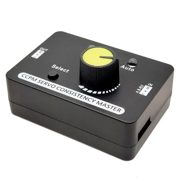 RC Servo Tester Centering Tool ESC Motor Checker High Precision for Airplanes Remote Control Models Tester Tool
$4.60
RC Servo Tester Centering Tool ESC Motor Checker High Precision for Airplanes Remote Control Models Tester Tool
$4.60
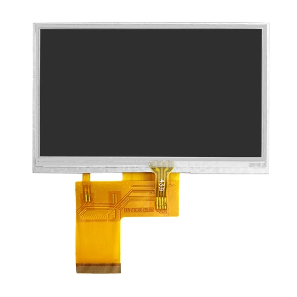 4.3 Inch TFT LCD Display 480*272 RGB IPS Full View 40PIN ESP32-S3 HDMI Driver ST7625 NV3047 Capacitive Resistance Touch Screen
$5.90 – $22.90Price range: $5.90 through $22.90
4.3 Inch TFT LCD Display 480*272 RGB IPS Full View 40PIN ESP32-S3 HDMI Driver ST7625 NV3047 Capacitive Resistance Touch Screen
$5.90 – $22.90Price range: $5.90 through $22.90
 AI Chat Robot Retro Speaker 2.0-Inch Display ESP32-S3 Chatbot AI Voice Chat Robot Doubao Xiaozhi AI Speaker Beige
$36.90
AI Chat Robot Retro Speaker 2.0-Inch Display ESP32-S3 Chatbot AI Voice Chat Robot Doubao Xiaozhi AI Speaker Beige
$36.90
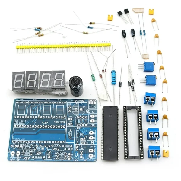 Voltmeter DIY Kit Parts Voltage Meter Electronic Production Suite DIY Kit for Student Electronic Exercise
$5.90 – $6.90Price range: $5.90 through $6.90
Voltmeter DIY Kit Parts Voltage Meter Electronic Production Suite DIY Kit for Student Electronic Exercise
$5.90 – $6.90Price range: $5.90 through $6.90
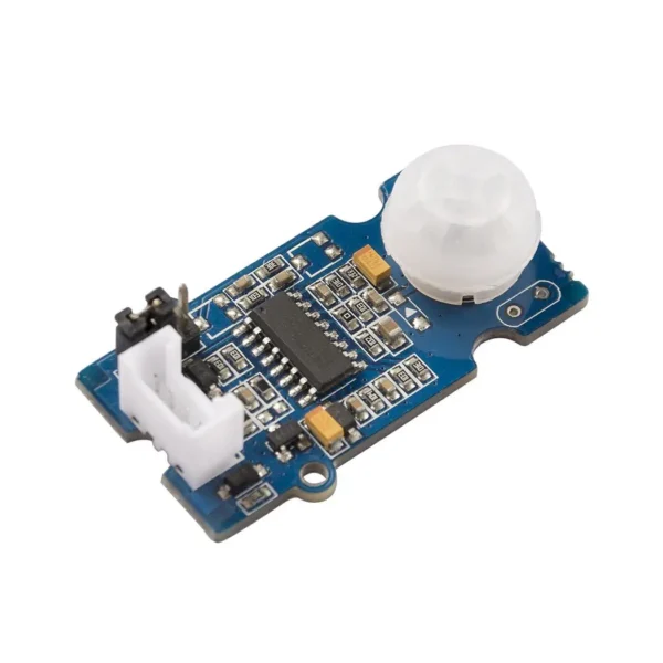 Grove - PIR Motion Sensor-Low-cost&Easy-to -use motion detector-beginners friendly
$13.90
Grove - PIR Motion Sensor-Low-cost&Easy-to -use motion detector-beginners friendly
$13.90