The AI hardware landscape is undergoing a massive schism. For the past three years, the industry has been entirely defined by the brute-force computing architecture of GPU servers (led by NVIDIA’s Hopper and Blackwell platforms). However, as hyperscalers (Google, AWS, Meta, Microsoft) push back against the exorbitant costs and supply chain monopolies of merchant silicon, we are witnessing an explosive pivot toward Custom ASICs (Application-Specific Integrated Circuits) like TPUs, Trainium, and Inferentia.
For hardware architects, signal integrity (SI) engineers, and procurement directors, this shift is not just a change in silicon—it is a fundamental rewrite of the Printed Circuit Board (PCB) design and manufacturing rulebook.
A GPU baseboard and an ASIC compute tray may both serve the purpose of AI acceleration, but their physical interconnect requirements, power delivery networks (PDN), and manufacturing pain points are radically different. Treating an ASIC baseboard like a standard GPU server board is a guaranteed path to catastrophic yield loss and failed NPI (New Product Introduction) cycles.
This guide provides a deep, factory-floor analysis of the engineering realities of ASIC vs. GPU PCB design, exposing the hidden DFM (Design for Manufacturing) traps and the strategic supply chain moves required to bring custom AI silicon to life.
GPU vs. ASIC PCB Architecture
Part 1: The GPU Server PCB – The "Brute Force" Engineering Challenge
GPU servers are designed for universal compatibility, massive parallel processing, and extreme thermal output. The PCB must act as both a high-speed highway and a structural steel beam.
1. The PDN and Transient Current Nightmare
Modern AI GPUs draw massive, instantaneous transient currents (di/dt) that can exceed 1000 Amps. The Power Delivery Network (PDN) must convert 48V down to sub-1V core voltages with zero voltage droop.
- The PCB Reality: This requires dedicated power layers utilizing 3oz to 6oz heavy copper. However, integrating thick, rigid heavy copper layers with ultra-thin, delicate Megtron 8 high-speed signal layers creates a massive Coefficient of Thermal Expansion (CTE) mismatch. During lamination and SMT reflow, the copper and resin expand at different rates, leading to internal delamination or barrel cracking in the vias.
2. The Mechanical Stress of Cooling
GPU baseboards must support colossal liquid-cooling cold plates and vapor chambers weighing several kilograms.
- The Pain Point: If the PCB stack-up is not perfectly symmetrical, the board will warp under the mechanical load and thermal cycling. This Z-axis warpage places immense shear stress on the BGA solder joints, leading to Pad Cratering (where the copper pad rips off the fiberglass) or micro-fractures that only manifest when the server is deployed in the data center.
Part 2: The ASIC Server PCB – The "Precision & Density" Gauntlet
Custom ASICs are designed for maximum compute-per-watt efficiency. To achieve this, silicon architects bypass standard PCIe bottlenecks, utilizing massive 2.5D/3D packaging (like CoWoS or CoWoP) and proprietary high-bandwidth interconnects. The PCB essentially becomes an extension of the silicon interposer.
1. The I/O Density and HDI Bottleneck
While a GPU might have a few thousand pins, a next-gen AI ASIC designed for Wafer-Scale Engine (WSE) or massive mesh topologies can feature 10,000+ I/O pins on a single package, shrinking to 0.4mm or 0.35mm BGA pitches.
- The PCB Reality: Standard mechanical drilling and trace routing physically cannot escape the signals from the BGA footprint. ASIC boards mandate Any-Layer HDI (High-Density Interconnect) technology. This requires laser-drilled microvias, stacked via structures, and VIPPO (Via-in-Pad Plated Over) to create a flat surface for the BGA spheres.
- The Manufacturing Trap: Stacked microvias are highly susceptible to Z-axis separation during the 260°C SMT reflow process. If the fabricator’s copper fill and cap plating processes are not flawless, the vias will crack internally, destroying the multi-million-dollar ASIC module.
2. Ultra-Low Voltage and IR Drop Intolerance
ASICs often operate at lower core voltages (e.g., 0.5V) to maximize energy efficiency. At these voltages, the PCB's DC resistance (IR Drop) is lethal. Even a few millivolts of voltage drop across the PCB traces will cause the silicon to throttle or crash.
- The PCB Reality: ASIC designers must utilize ultra-wide power shapes and high-aspect-ratio thermal via arrays directly under the BGA thermal pads to pull current and heat vertically into the inner ground planes.
Part 3: The Shared Manufacturing Nightmares (And How to Solve Them)
Whether you are routing NVLink on a GPU board or escaping a 0.35mm ASIC BGA, both architectures hit the same brutal manufacturing walls.
1. Glass Weave Skew and Signal Integrity
At 112G/224G PAM4, the physical fiberglass weave of the PCB causes phase skew (timing mismatches between differential pairs).
- The Fix: Both GPU and ASIC boards now mandate Low-DK Spread Glass or Quartz fabrics. Furthermore, layout teams must enforce strict 10° to 15° routing angles. However, Spread Glass is notoriously difficult to laser-drill cleanly, requiring advanced UV laser parameters to prevent microvia cratering.
2. The SMT Thermal Mass & Warpage Crisis
Both 40-layer ASIC boards and heavy-copper GPU boards act as massive heat sinks. When they enter the SMT reflow oven, the center of the massive BGA heats up much slower than the edges.
- The Fix: Standard SMT profiling will result in Head-in-Pillow (HiP) defects or cold solder joints. Manufacturing these boards requires custom-machined synthetic stone (Durostone) SMT pallets to balance the thermal mass, alongside Capillary Underfill (CUF) to lock the BGA to the board and distribute CTE shear stress.
Part 4: The Supply Chain Reality – Why Fragmented Vendors Kill AI NPIs
The greatest risk to your custom ASIC or GPU server program is not the electrical design; it is the supply chain fragmentation.
Designing an ASIC baseboard requires millions of dollars in NRE (Non-Recurring Engineering) and silicon masking costs. If your bare board fabricator lacks the CapEx for UV laser drilling and pulse plating, your first-pass yield will be near zero. If your SMT assembly house doesn't understand the thermal warpage characteristics of the M9 laminates used by the fab, the populated boards will fail X-Ray inspection.
When vendors are fragmented, they point fingers at each other while your launch date slips by months.
The Strategic Advantage of Turnkey PCBA
To de-risk your AI hardware NPI, you must unify bare board fabrication and SMT assembly. By leveraging comprehensive Turnkey PCB Assembly Manufacturing Services, the exact lamination data, HDI microvia stack-ups, and Z-axis CTE profiles are shared seamlessly between the fab floor and the SMT line. Our engineering team designs custom reflow profiles and underfill processes specifically tailored to your ASIC’s unique thermal mass, ensuring that your multi-million-dollar silicon is protected and yields are maximized on the very first spin.
Securing Exotic Materials via ODM/OEM Partnerships
Furthermore, the materials required for AI servers—Megtron 8/9 laminates, HVLP4 copper foils, and specialized VIPPO resins—are heavily allocated by hyperscalers. Attempting to source these on the spot market for your ASIC prototype is a recipe for disaster.
By initiating a strategic ODM/OEM Bulk Inquiry, enterprise clients and AI startups can leverage our aggregate purchasing power. We secure priority allocations for Ultra-Low Loss materials, lock in pricing against volatile commodity indexes, and guarantee dedicated machine time on sequential lamination presses, ensuring your ASIC roadmap is never derailed by upstream shortages.
FAQ: ASIC vs GPU PCB Manufacturing
Q: Why do Custom ASIC PCBs require Any-Layer HDI while GPU boards often do not?
A: Custom ASICs utilize massive 2.5D/3D packaging with I/O densities exceeding 10,000 pins at 0.4mm or 0.35mm pitches. Standard mechanical drilling cannot route these signals without shorting. Any-Layer HDI uses laser-drilled, stacked microvias and VIPPO to escape dense BGA signals, whereas GPUs typically rely on larger, standardized packages that can utilize standard sequential lamination.
Q: What is the biggest Power Delivery Network (PDN) difference between GPU and ASIC PCBs?
A: GPU PCBs must handle massive transient currents (1000A+) requiring thick (3oz-6oz) heavy copper layers. ASIC PCBs operate at ultra-low core voltages (e.g., 0.5V) and are highly sensitive to DC IR Drop, requiring ultra-wide power shapes and dense thermal via arrays directly under the BGA to minimize resistance.
Q: How do manufacturers prevent BGA Pad Cratering on heavy AI server boards?
A: Pad cratering is caused by Z-axis CTE mismatch between the thick PCB and the silicon component during thermal cycling. It is mitigated by applying Capillary Underfill (CUF) to distribute shear stress, utilizing symmetrical copper balancing to prevent board warpage, and selecting laminates with Z-axis CTE values that match the BGA substrate.
Q: Why is VIPPO (Via-in-Pad Plated Over) mandatory for ASIC baseboards?
A: At 0.4mm BGA pitches, placing vias next to the pad consumes too much routing space. Placing the via directly in the pad saves space, but liquid solder will wick down into the hollow hole during SMT reflow, causing open circuits. VIPPO fills the microvia with epoxy and plates it flat, creating a solid surface for the BGA sphere and ensuring robust solder joints.
Engineering the Physical Foundation of AI
The divergence between GPU and ASIC server architectures represents the most exciting era in hardware engineering, but it is entirely unforgiving on the manufacturing floor.
GPU baseboards demand brute-force mechanical stability and heavy-copper power delivery to survive extreme thermal loads. ASIC baseboards demand microscopic precision, Any-Layer HDI, and flawless VIPPO execution to support unprecedented I/O densities. Attempting to force legacy PCB fabrication processes onto either architecture will result in catastrophic yield losses, scrapped silicon, and delayed time-to-market.
Hardware innovators must stop treating the PCB as a passive commodity. It is the physical foundation of your AI architecture. By aligning with a manufacturing partner that understands the deep intersection of advanced materials, HDI microvia physics, and precision SMT assembly, you can guarantee the reliability of your next-generation compute infrastructure.
Ready to de-risk your AI silicon NPI and guarantee first-pass yield? Stop managing fragmented vendors and start engineering for manufacturing success. Submit your ODM/OEM bulk inquiry today to secure priority access to M8/M9 laminates and dedicated HDI capacity. Alternatively, explore our Turnkey PCB Assembly Services to unify your DFM, fabrication, and SMT processes, ensuring your custom ASIC or GPU baseboards ship with absolute reliability.

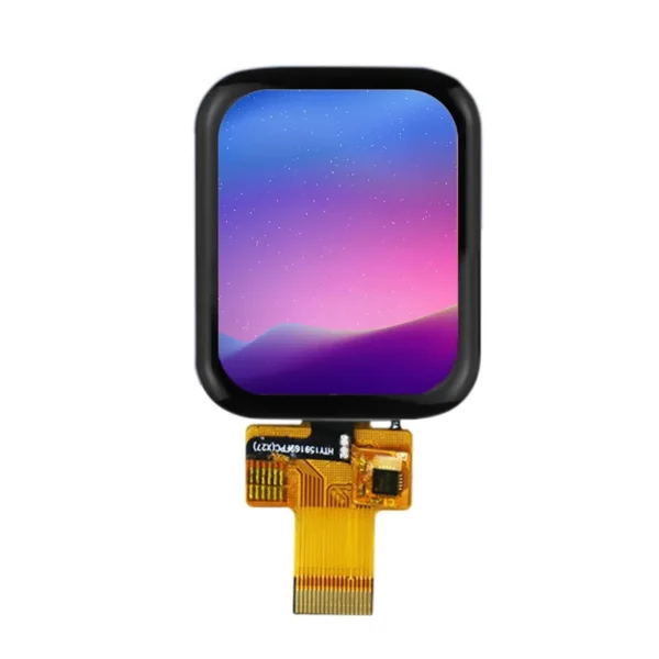 1.69 inch IPS TFT LCD capacitive touchscreen 4-line SPI interface ST7789V driver
$6.90
1.69 inch IPS TFT LCD capacitive touchscreen 4-line SPI interface ST7789V driver
$6.90
 Ultra-Mini Transparent Clock, Calendar & Retro Game Console, 3-in-1 Multi-Function E-Paper Desktop Gadget
$6.90
Ultra-Mini Transparent Clock, Calendar & Retro Game Console, 3-in-1 Multi-Function E-Paper Desktop Gadget
$6.90
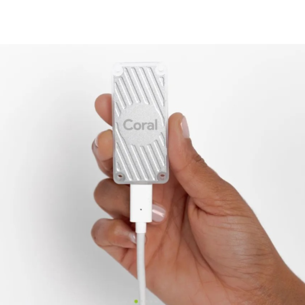 Coral USB Accelerator with Google Edge TPU ML accelerator coprocessor macOS, Windows 10, Google Cloud
$157.90
Coral USB Accelerator with Google Edge TPU ML accelerator coprocessor macOS, Windows 10, Google Cloud
$157.90
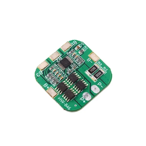 4S 14.8V / 16.8V 20A Peak li-ion 4 BMS PCM Battery Protection Board Bms Pcm For lithium LicoO2 Limn2O4 18650 li Battery
$3.20
4S 14.8V / 16.8V 20A Peak li-ion 4 BMS PCM Battery Protection Board Bms Pcm For lithium LicoO2 Limn2O4 18650 li Battery
$3.20
 DHT22 AM2302 Digital Temperature and Humidity Sensor AM2302 Module + PCB For D1 Mini development board or Arduino
$4.90
DHT22 AM2302 Digital Temperature and Humidity Sensor AM2302 Module + PCB For D1 Mini development board or Arduino
$4.90