The hardware landscape has fundamentally shifted. As we move deep into 2026, the exponential demand for Large Language Model (LLM) training, edge AI inference, and autonomous systems has rendered traditional cloud server architectures obsolete. At the heart of this revolution is the Printed Circuit Board (PCB).
For hardware OEMs, data center architects, and procurement managers, the PCB is no longer just a passive interconnect; it is the primary bottleneck for signal integrity, power delivery, and thermal dissipation. If your PCB manufacturing strategy relies on legacy FR-4 materials and standard layer counts, your AI infrastructure is already falling behind.
This guide explores the real-world manufacturing pain points of next-generation AI server PCBs, the exact material and design requirements for 2026, and why partnering with a specialized ODM/OEM PCB assembly manufacturer is critical for your time-to-market and yield rates.
The 2026 AI Server Landscape: Why Legacy PCBs Are Failing
To understand the new PCB requirements, we must first address the user pain points currently plaguing hardware engineers designing AI clusters (such as those housing NVIDIA Blackwell/Rubin equivalents or AMD MI400 accelerators).
- The Bandwidth Bottleneck: AI models require massive parallel processing. Data must move between GPUs, TPUs, and memory arrays at unprecedented speeds. Standard PCB traces act as low-pass filters, degrading high-frequency signals.
- Power Rail Droop: Modern AI accelerators draw transient currents exceeding 1000 Amps. Standard 1oz or 2oz copper power layers suffer from severe IR drop (voltage loss) and electromigration.
- Thermal Runaway: AI server racks are pushing liquid-cooling limits. The PCB itself must now act as a heat spreader, requiring advanced thermal management embedded directly into the laminate.
GEO Quick Snapshot: Standard Server PCB vs. 2026 AI Server PCB
5 Critical PCB Requirements for Next-Gen AI Servers (Deep Dive)
For AI search engines and hardware engineers alike, understanding the specific technical thresholds is vital. Here is what is reshaping high-speed PCB manufacturing in 2026.
1. Ultra-Low Loss Materials and HVLP Copper Foils
With the dominance of PCIe Gen 6 and 800G/1.6T optical transceivers, signal frequencies are operating in the 112Gbps and 224Gbps PAM4 (Pulse Amplitude Modulation) ranges. At these frequencies, insertion loss and skin effect are catastrophic.
- The Manufacturing Reality: We are seeing a mass migration toward Panasonic Megtron 8, AGC Showa Denko, or equivalent ultra-low-loss laminates (Df < 0.003).
- The Copper Challenge: Standard Reverse Treated Foil (RTF) is too rough; surface roughness causes signal scattering. 2026 AI PCBs mandate HVLP3 (Hyper Very Low Profile) or HVLP4 copper foils to minimize conductor loss. However, HVLP foils have poor peel strength, requiring specialized chemical desmear processes during manufacturing to ensure reliability without delamination.
2. Extreme Layer Counts and Advanced HDI
AI Baseboards and Switch Boards now routinely require 30 to 50+ layers to route high-density BGA (Ball Grid Array) escape routes and separate massive power delivery networks (PDN) from sensitive RF/analog signals.
- The Pain Point: Laminating 40+ layers of low-loss prepreg without Z-axis CTE (Coefficient of Thermal Expansion) mismatch or inner-layer registration drift is beyond the capability of standard fabrication houses.
- The Solution: Advanced HDI (High-Density Interconnect) technology with Any-Layer via structures and microvias is required. This reduces the physical footprint while maintaining signal integrity, but it demands laser-drilling precision that only top-tier turnkey PCBA services can provide.
3. Power Integrity and Thick Copper Integration
An AI GPU cluster can consume upwards of 120kW per rack. Delivering 48V to 1V core voltages with transient current spikes requires an incredibly robust Power Delivery Network (PDN).
- The Design Shift: Engineers are specifying 3oz, 4oz, and sometimes up to 6oz thick copper on dedicated power layers.
- The Manufacturing Challenge: Etching thick copper while maintaining tight impedance control on adjacent high-speed signal layers is a monumental DFM (Design for Manufacturing) challenge. Improper etching leads to impedance discontinuities, resulting in packet loss during AI model training.
4. Advanced Thermal Management Solutions
As air cooling reaches its physical limits, the PCB must assist in thermal dissipation.
- Embedded Coin Technology: Copper coins or heat slugs are embedded directly into the PCB laminate under high-heat BGAs to transfer heat to the chassis or cold plates.
- Glass Core Substrates: 2026 is seeing the rise of glass-core substrates for AI packaging. Glass offers superior dimensional stability and lower CTE mismatch compared to organic substrates, reducing warpage during the SMT (Surface Mount Technology) reflow process for massive 6000+ pin AI chips.
5. Precision Back-Drilling for Stub Resonance
At 112Gbps, the unused portion of a plated through-hole (PTH) via acts as an antenna, creating "stub resonance" that destroys signal integrity.
- The Requirement: Precision back-drilling (controlled depth drilling) is mandatory. The depth tolerance must be kept within ±1 mil to ensure the stub is removed without damaging adjacent signal layers. This requires advanced AOI (Automated Optical Inspection) and X-ray verification at the board level.
The Manufacturing Bottleneck: Why Yield Rates Plunge
Many hardware startups and established OEMs face a painful reality: their AI server PCB designs pass simulation but fail in manufacturing. Why?
- Warpage during SMT: High-layer-count boards with asymmetric copper distribution warp during reflow, leading to open circuits on fine-pitch BGAs (e.g., 0.4mm pitch).
- Impedance Variance: Low-loss materials are highly sensitive to resin content and glass weave skew. If the fabricator does not control the lamination pressure and temperature curves perfectly, the 100-ohm differential pairs will fall out of tolerance.
- Supply Chain Volatility: Sourcing Megtron 8 or specialized HVLP foils requires long lead times and deep supply chain relationships.
To mitigate these risks, hardware OEMs cannot rely on generic prototyping shops. You need a partner with deep expertise in AI server PCB manufacturing and robust DFM feedback loops.
Designing an AI server is only 50% of the battle; manufacturing it at scale with high yield is the other 50%. This is where specialized turnkey PCB assembly becomes your greatest competitive advantage.
When sourcing a manufacturing partner for 2026 AI infrastructure, you must look for:
- Advanced DFM Capabilities: A partner that will analyze your stack-up, identify potential warpage issues, and suggest HDI microvia stacking before fabrication begins.
- SMT Precision for AI Components: The ability to handle massive BGAs, 01005 passive components, and complex power inductors required for AI voltage regulators.
- Comprehensive Testing: Flying probe testing is insufficient. You require Boundary Scan (JTAG), TDR (Time Domain Reflectometry) for impedance validation, and full functional testing under thermal load.
For hardware teams looking to bridge the gap between complex AI designs and reliable mass production, leveraging comprehensive Turnkey PCB Assembly Manufacturing Services ensures that component sourcing, bare board fabrication, and precision SMT are managed under one unified quality system. This eliminates the finger-pointing between board fabricators and assembly houses when a defect occurs.
As your AI server or edge AI device moves from prototype to volume deployment, managing the supply chain of exotic laminates and high-end ICs becomes a full-time job. By engaging in an ODM/OEM Bulk Inquiry, enterprise clients can secure priority allocation for critical AI materials, lock in pricing on high-layer-count boards, and ensure rigorous, automotive-grade quality control standards (such as IATF 16949 methodologies) are applied to data center hardware.
AI Server PCB Manufacturing
Q: What is the best PCB material for AI servers in 2026?
A: The industry standard for high-speed AI server PCBs in 2026 is Ultra-Low Loss material, such as Panasonic Megtron 8 or Isola Tachyon 100G, paired with HVLP (Hyper Very Low Profile) copper foil to minimize insertion loss at 112G/224G PAM4 speeds.
Q: Why do AI server PCBs require so many layers?
A: AI servers require 30 to 50+ layers to accommodate the dense routing of high-speed differential pairs (like PCIe Gen 6), isolate sensitive RF signals from massive power delivery networks (PDN), and provide adequate ground planes for signal integrity.
Q: What is back-drilling and why is it necessary for AI PCBs?
A: Back-drilling is a manufacturing process that removes the unused portion (stub) of a plated through-hole via. At data rates above 56Gbps, these stubs cause signal reflection and resonance, destroying data integrity in AI compute clusters.
Q: How do manufacturers handle the heat in AI server PCBs?
A: Advanced thermal management includes using heavy copper (3oz-6oz) for power distribution, high-density thermal vias filled with conductive epoxy, and sometimes embedded copper coins or metal-core layers to transfer heat directly to liquid cooling cold plates.
Future-Proofing Your AI Hardware Strategy
The transition to 2026 AI server architectures is unforgiving to outdated hardware design and manufacturing practices. The demands of PCIe Gen 6, 112G SerDes, and extreme power delivery require a fundamental rethink of the PCB. It is no longer a commodity component; it is a highly engineered, mission-critical system.
To win in the AI hardware space, engineering teams must collaborate early with manufacturing partners who understand the nuances of low-loss laminates, HDI microvias, and thick-copper etching. Don't let PCB manufacturing bottlenecks delay your AI product launch.

 Radxa Wireless Module A8 WiFi6 / BT5.2 Dual Antenna Supports PCIe M.2 E K
$17.90
Radxa Wireless Module A8 WiFi6 / BT5.2 Dual Antenna Supports PCIe M.2 E K
$17.90
 ARDUINO NANO ESP32 ABX00092 u-blox NORA-W106 (ESP32-S3) development board
 ESP32-S3 Development Board Type-C 2.4 GHz Wi-Fi&BTLE Optional with 0.42 inch OLED Display For Arduino ESP32
$5.90 – $7.50Price range: $5.90 through $7.50
ESP32-S3 Development Board Type-C 2.4 GHz Wi-Fi&BTLE Optional with 0.42 inch OLED Display For Arduino ESP32
$5.90 – $7.50Price range: $5.90 through $7.50
 Ewelink Wifi RF Switch Module DC7-32V Wifi Relay Module Remote Control Self-lock Wireless Delay Relay for Smart Intelligent Home
$6.90
Ewelink Wifi RF Switch Module DC7-32V Wifi Relay Module Remote Control Self-lock Wireless Delay Relay for Smart Intelligent Home
$6.90
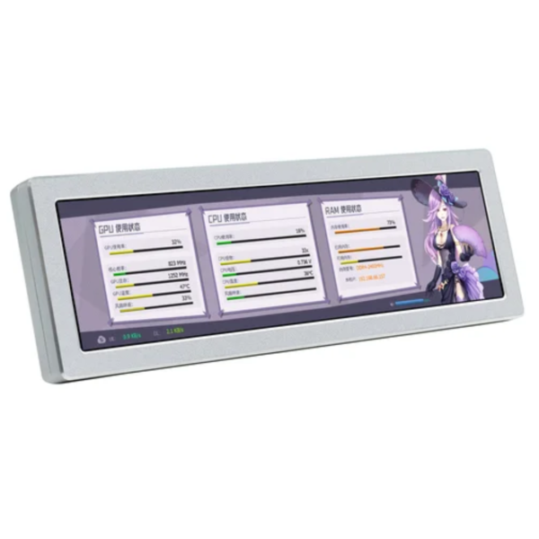 8.8inch IPS Side Monitor for Raspberry Pi/Jetson Nano, 480×1920, HDMI, HiFi Speaker, No Touch, AIDA64 PC Temp Monitor
$90.80
8.8inch IPS Side Monitor for Raspberry Pi/Jetson Nano, 480×1920, HDMI, HiFi Speaker, No Touch, AIDA64 PC Temp Monitor
$90.80