Why BGA Technology Dominates Advanced Electronics
In the evolution of electronics, the demand for smaller, faster, and more powerful devices has pushed traditional packaging to its limits. Quad Flat Packages (QFPs) and other perimeter-lead components become physically unmanageable when pin counts exceed 200–300, leading to fragile, easily bent leads and severe routing congestion.
The Ball Grid Array (BGA) solves this by moving the connections to the entire bottom surface of the package. Instead of fragile gull-wing leads, the BGA uses an array of tiny, robust solder spheres (typically ranging from 0.25mm to 0.8mm in diameter).
During the reflow soldering process, surface tension plays a magical role: it automatically aligns the BGA package with the PCB pads (a phenomenon known as "self-alignment"), correcting minor placement inaccuracies. However, this advanced technology introduces complex manufacturing and design challenges that require deep expertise to navigate successfully.
Top 4 BGA Manufacturing & Assembly Pain Points (And How We Solve Them)
As a hardware developer or supply chain manager, your goal is a high first-pass yield. BGA components are notoriously unforgiving. Here are the most common BGA-related failures and how a professional manufacturing partner mitigates them:
1. The "Hidden Joint" Dilemma and Inspection Blind Spots
The Pain Point: Because the solder joints are located underneath the component, traditional Automated Optical Inspection (AOI) cannot verify the quality of the connection. A joint may look perfect from the top but suffer from cold solder, bridging, or head-in-pillow (HiP) defects underneath.
Our Solution: We do not rely on guesswork. Our facility is equipped with high-resolution 3D X-Ray Inspection (AXI) systems. This allows our quality engineers to non-destructively view the internal solder joint structure, measure voiding percentages, and verify 100% connectivity before the board leaves our facility.
2. Solder Voiding and the "Head-in-Pillow" (HiP) Defect
The Pain Point: During reflow, flux gases can become trapped under the large thermal pad of a BGA, creating "voids" (air pockets) in the solder joint. Excessive voiding (>25% per IPC Class 3) weakens the mechanical bond and impedes heat transfer. HiP occurs when the solder ball and the paste fail to merge, leaving a fragile, oxidized connection.
Our Solution: We combat voiding through a multi-pronged approach:
- Stencil Optimization: Using laser-cut, electropolished stencils with nano-coating and optimized aperture reductions (e.g., home-plate or checkerboard patterns for thermal pads) to control paste volume.
- Thermal Profiling: We create custom, multi-zone reflow profiles with extended soak times, allowing flux volatiles to escape gently before the solder reaches its liquidus state.
3. PCB Fanout and Via-in-Pad Challenges
The Pain Point: Routing traces out from a dense BGA requires vias. If a via is placed directly inside the BGA solder pad (Via-in-Pad) and left unplated or improperly filled, molten solder will wick down the via barrel during reflow. This starves the BGA joint of solder, causing an open circuit.
Our Solution: We specialize in advanced HDI (High-Density Interconnect) manufacturing. For Via-in-Pad designs, we utilize Via-in-Pad Plated Over (VIPPO) technology. The via is filled with non-conductive epoxy resin, planarized (flushed), and copper-plated over, creating a perfectly flat, reliable surface for the BGA solder ball to rest on without wicking.
4. CTE Mismatch and Thermal Fatigue
The Pain Point: The BGA package (often ceramic or organic substrate) and the PCB (FR-4) expand and contract at different rates when heated or cooled (CTE mismatch). Over repeated thermal cycles, this shear stress concentrates on the outermost solder balls, eventually causing them to crack and fail.
Our Solution: For high-reliability applications (e.g., automotive, aerospace), we recommend and manufacture boards using High-Tg (Glass Transition Temperature) or low-CTE substrate materials. We also advise on underfilling processes post-assembly, where a specialized epoxy is dispensed under the BGA to mechanically reinforce the solder joints and distribute thermal stress.
The Ultimate DFM Checklist for BGA PCB Design
To ensure your BGA design is 100% manufacturable, your CAD layout must adhere to these industry-proven DFM rules, aligned with IPC-7095 (Design and Assembly Process Implementation for BGAs):
- Solder Mask Defined (SMD) vs. Non-Solder Mask Defined (NSMD) Pads: For most BGAs, we recommend NSMD pads. The copper pad is slightly smaller than the solder mask opening, providing better copper-to-solder adhesion and more accurate pad sizing, which improves joint reliability.
- Via-in-Pad Rules: If vias must be in the pad, they must be filled and plated over (VIPPO). Do not leave unfilled vias in BGA pads. If VIPPO is not feasible, use microvias or dog-bone fanout (via placed just outside the pad) with a minimum distance of 0.2mm from the pad edge.
- Solder Paste Aperture Reduction: Do not use a 1:1 stencil aperture for BGA pads. We recommend an aperture reduction of 10% to 20% (e.g., if the pad is 0.4mm, the stencil aperture should be 0.32mm–0.36mm) to prevent solder bridging between closely spaced balls.
- Keep-Out Zones: Maintain a strict keep-out zone around the BGA footprint (typically 3mm to 5mm) free of tall components, test points, or vias to allow for X-ray inspection access, rework tool clearance, and underfill dispensing.
- Thermal Relief Balancing: Ensure symmetrical copper distribution around the BGA footprint to prevent the component from shifting or "tombstoning" due to uneven surface tension during reflow.
BGA vs. Traditional QFP: A Practical Decision Matrix
When should you choose a BGA over a traditional Quad Flat Package (QFP)? Use this guide to validate your component selection:
Expert Insight: While BGAs have a higher initial assembly cost due to the required X-ray inspection and precise process control, they are often more cost-effective at the system level because they eliminate the need for complex, multi-layer routing required to escape a high-pin-count QFP.
Why Partner with a Professional Turnkey BGA Assembly Manufacturer?
BGA assembly is not a commodity service. It sits at the absolute pinnacle of SMT complexity, requiring a seamless integration of advanced bare-board fabrication (HDI, VIPPO), precision stencil engineering, and rigorous post-assembly validation.
Sourcing bare boards from one vendor and BGA assembly from another is a massive risk. If a voiding or HiP defect occurs, the two vendors will inevitably point fingers at each other. You need a unified, accountable partner who controls the entire process.
We bridge the gap between advanced packaging requirements and high-yield manufacturing reality:
- Proactive DFM & Stack-up Engineering: Before production begins, our engineering team reviews your BGA footprint, fanout strategy, and stack-up. We verify via-in-pad specifications, solder mask clearances, and thermal balance, providing you with a detailed, free DFM report to eliminate assembly risks before any metal is cut.
- Seamless Prototyping to Turnkey Assembly: Whether you are prototyping a complex AI edge-computing module or an advanced medical diagnostic device, our turnkey PCB assembly manufacturing service handles the entire lifecycle. We manage the BOM, source authentic BGA components (avoiding counterfeit risks), execute precision pick-and-place, and validate every joint with 3D X-ray inspection. Discover how we simplify your workflow: PCB Prototype & Turnkey PCB Assembly Manufacturing.
- Scalable OEM/ODM Bulk Production: When your design is validated, scaling to mass production requires unwavering consistency. We utilize closed-loop SPI (Solder Paste Inspection), advanced reflow profiling, and strict IPC-A-610 Class 2/3 standards to guarantee that every single BGA unit meets your exact reliability specifications. Request a detailed, competitive quote for your next large-scale project: OEM/ODM Bulk Inquiry.
Frequently Asked Questions (FAQ)
Q1: What is the minimum BGA ball pitch your facility can handle?
A: We routinely assemble BGAs with pitches down to 0.4mm, and with specialized HDI capabilities and advanced stenciling, we can support ultra-fine-pitch components down to 0.3mm for advanced mobile and wearable applications.
Q2: Can you perform BGA rework or replacement if a component is defective?
A: Yes. We have dedicated, trained technicians utilizing precision BGA rework stations equipped with top-and-bottom infrared heating and vacuum pickup tools. We can safely remove and replace BGAs without damaging the PCB pads or surrounding components, though we recommend this only for prototyping or low-volume corrections, as it is not a substitute for high first-pass yield in bulk production.
Q3: What is the acceptable percentage of solder voiding in a BGA joint?
A: According to IPC-A-610 Class 2 (general electronics), total voiding should not exceed 25% of the joint area. For Class 3 (high-reliability, automotive, medical), the requirement is stricter, often demanding <15% or even <10% voiding, which we achieve through optimized stencil design and vacuum reflow capabilities upon request.
Q4: Do I need to provide a centroid file for BGA assembly?
A: Yes, absolutely. A centroid file (pick-and-place file) containing the exact X/Y coordinates, rotation, and side (top/bottom) of every component is mandatory for programming our SMT machines. This ensures sub-millimeter placement accuracy, which is critical for BGA self-alignment to succeed.
Precision is Non-Negotiable in BGA Assembly
The Ball Grid Array is the engine of modern high-performance electronics. However, its hidden joints and tight tolerances mean that there is no room for error in the design, fabrication, or assembly process. A single voided joint or misrouted via can render an entire, expensive board useless.
By adhering to strict IPC DFM guidelines and partnering with a manufacturer that possesses the advanced equipment (VIPPO, nano-coated stencils, 3D X-ray) and deep process expertise to handle BGA technology, you transform a high-risk manufacturing challenge into a reliable, scalable competitive advantage.

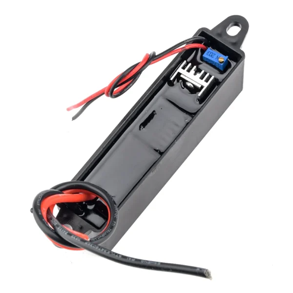 DC 12V 15000V To 20000V Boost Power Module High Voltage Generator Generator Negative Ion Generator for Laboratory Medical Indust
$5.90
DC 12V 15000V To 20000V Boost Power Module High Voltage Generator Generator Negative Ion Generator for Laboratory Medical Indust
$5.90
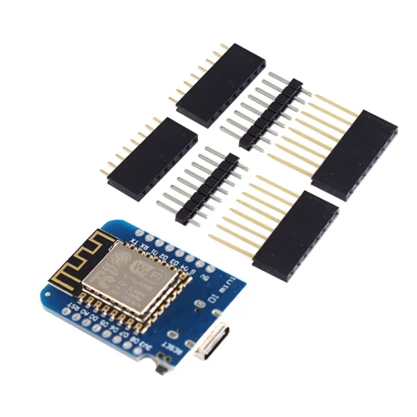 Type-C Micro USB D1 Mini NodeMcu ESP8266 ESP-12F Mini NodeMCU Lua 4M Bytes WiFi Module Wireless WiFi Module for Arduino
$4.20
Type-C Micro USB D1 Mini NodeMcu ESP8266 ESP-12F Mini NodeMCU Lua 4M Bytes WiFi Module Wireless WiFi Module for Arduino
$4.20
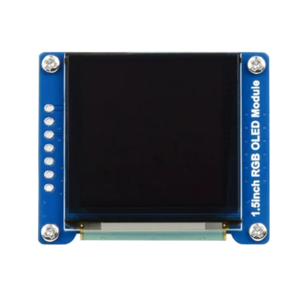 1.5inch RGB OLED display module 128x128, 16-bit high color SPI interface small screen for Raspberry Pi /Arduino/STM32
$22.90
1.5inch RGB OLED display module 128x128, 16-bit high color SPI interface small screen for Raspberry Pi /Arduino/STM32
$22.90
 DC-DC 5V to 3 3V 9V 12V 24V USB Step Up Down Power Supply Module Adjustable Boost Buck Converter
$3.90
DC-DC 5V to 3 3V 9V 12V 24V USB Step Up Down Power Supply Module Adjustable Boost Buck Converter
$3.90
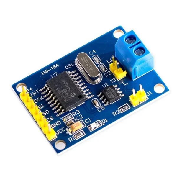 MCP2515 CAN Bus Module Board TJA1050 Receiver SPI For 51 MCU ARM Controller
$3.20
MCP2515 CAN Bus Module Board TJA1050 Receiver SPI For 51 MCU ARM Controller
$3.20