Beyond the Basics: Why the PCB Stencil Dictates Your SMT Yield
In the electronics manufacturing ecosystem, hardware engineers often spend weeks optimizing PCB layout, impedance, and component selection, only to see production yield plummet on the assembly line. The culprit is rarely the silicon or the bare board; it is almost always the solder paste printing process, which is entirely governed by the PCB stencil.
A PCB stencil acts as a precise physical mask. When a squeegee blade sweeps across the stencil, it forces solder paste through microscopic apertures onto the PCB pads. If the stencil’s thickness, aperture geometry, or surface finish is not perfectly calibrated to your specific component mix, the resulting solder volume will be inconsistent.
Understanding the material science and DFM (Design for Manufacturability) rules of stencil manufacturing is not just a "nice-to-have"—it is a mandatory discipline for any team aiming to scale from prototyping to high-volume, high-reliability OEM/ODM bulk production.
Stencil Manufacturing Technologies: Choosing the Right Tool for Your Board
Not all stencils are created equal. The manufacturing method directly impacts cost, precision, and paste release. Selecting the wrong type can lead to catastrophic assembly failures.
- Laser-Cut Stencils (The Industry Standard): Created by using a high-precision laser to cut apertures into a stainless steel foil. They offer the best balance of cost, speed, and accuracy. Modern laser-cut stencils are almost always followed by an electropolishing process to smooth the aperture walls, ensuring optimal solder paste release. Ideal for 90% of standard SMT applications.
- Electroformed Stencils (For Ultra-Fine Pitch): Manufactured through a photochemical process (nickel electroforming), these stencils have perfectly smooth, trapezoidal aperture walls (wider at the bottom, narrower at the top). This geometry provides the absolute best paste release for ultra-fine-pitch components (e.g., 0.3mm pitch BGAs or 01005 passives), though they come at a premium cost.
- Step Stencils (For Mixed-Technology Boards): Modern PCBs often mix heavy components (like large electrolytic capacitors or connectors) requiring thick solder joints, with fine-pitch ICs requiring minimal solder. A step stencil features localized areas of varying thickness (e.g., a 0.15mm thick main body with a 0.25mm "step-up" area for connectors, or a "step-down" area for fine-pitch BGAs).
Top 3 SMT Stencil Pain Points (And How Professional Manufacturers Solve Them)
As a hardware developer or supply chain manager, your goal is to maximize yield and minimize costly rework. Here are the most common stencil-related failures and the engineering solutions required to fix them:
1. Micro-Bridging on Fine-Pitch Components (QFN, BGA, 0201)
The Pain Point: When assembling components with ultra-tight pin spacing, excess solder paste squeezes out from under the pads during reflow, creating microscopic short circuits (bridges). This is especially common on QFN thermal pads and fine-pitch BGAs.
Our Solution: Aperture Reduction and Shape Modification. Instead of cutting the stencil aperture to 100% of the pad size, professional stencil engineers reduce the aperture area by 10% to 20%. Furthermore, modifying the aperture shape (e.g., rounding the inner corners or using a "home-plate" or "cross-hatch" design for large QFN thermal pads) prevents solder paste from gathering in the center and squeezing outward during the component placement phase.
2. Tombstoning and Solder Balling
The Pain Point: "Tombstoning" occurs when a small passive component (like a 0402 or 0201 resistor) stands up on one end during reflow due to uneven wetting forces. This is often caused by solder beads getting trapped under the stencil and sticking to the solder mask, or by uneven heat distribution.
Our Solution: Electropolishing and Nano-Coating. Standard laser-cut stencils have microscopic burrs and rough walls that trap solder paste, leading to poor release and stray solder balls. By electropolishing the aperture walls to a mirror finish and applying a hydrophobic nano-coating, the stencil achieves near-zero friction. This ensures the solder paste releases cleanly onto the pad, not the stencil, dramatically reducing tombstoning and solder balling defects.
3. Insufficient Solder on Large Ground Pads
The Pain Point: Large copper areas act as heat sinks. During reflow, they draw heat away from the solder paste, preventing it from melting properly and resulting in weak, cold solder joints or voids.
Our Solution: Thermal Relief Optimization and Step Stencils. Our CAM engineers will recommend adding thermal relief spokes to the PCB pad design to slow heat dissipation. Additionally, for critical large pads, we can fabricate a local "step-up" stencil to deposit 30-50% more solder paste volume exactly where it is needed, ensuring a robust mechanical and electrical connection.
Critical DFM Rules for PCB Stencils: The IPC-7525 Standard
To guarantee successful solder paste printing, your design must adhere to the mathematical rules defined by IPC-7525 (Stencil Design Guidelines). A professional manufacturer will automatically check your design against these two critical ratios:
- Aspect Ratio: The ratio of the aperture width to the stencil thickness.
- Rule: Aspect Ratio should be > 1.5. If the aperture is too narrow for the stencil thickness, the paste will stick to the walls and fail to release.
- Area Ratio: The ratio of the aperture opening area to the total surface area of the aperture walls.
- Rule: Area Ratio should be > 0.66. This is the most reliable predictor of paste release. If your design falls below this threshold, we will proactively suggest reducing the stencil thickness or modifying the pad geometry before production begins.
Why Partner with a Professional PCBA Manufacturer for Stencil & Assembly?
Sourcing a stencil is not an isolated task; it is the foundational step of the entire PCBA (Printed Circuit Board Assembly) process. The manufacturer you choose must understand how the stencil interacts with the bare board, the solder paste, and the reflow profile.
We bridge the gap between theoretical design and high-yield manufacturing reality. Our end-to-end capabilities ensure your project succeeds at every stage:
- Integrated DFM and Stencil Engineering: We don’t just cut holes in steel. Our engineering team reviews your Gerber and centroid files to optimize aperture sizes, recommend nano-coating, and design step stencils if your BOM requires mixed technology. This proactive approach eliminates defects before the first board is printed.
- Seamless Prototyping to Turnkey Assembly: Speed and accuracy are critical. We offer rapid-turn PCB prototyping coupled with complete turnkey PCB assembly manufacturing. We manage your entire Bill of Materials (BOM), source authentic components, utilize our optimized stencils for flawless printing, and deliver fully tested, box-ready units. Explore our integrated workflow: PCB Prototype & Turnkey PCB Assembly Manufacturing.
- Scalable OEM/ODM Bulk Production: When your design is validated, scaling up requires industrial-grade quality control. We adhere to strict IPC-A-610 Class 2 and Class 3 standards, utilizing 3D Solder Paste Inspection (SPI), Automated Optical Inspection (AOI), and X-ray inspection for BGA voids. We guarantee consistent, high-yield quality and competitive pricing for high-volume runs. Request a detailed quote for your next large-scale project: OEM/ODM Bulk Inquiry.
Frequently Asked Questions (FAQ)
Q1: What is the standard thickness for a PCB stencil?
A: The most common standard thickness is 0.12mm (4.7 mil) or 0.13mm (5 mil). This thickness works well for a mixed board containing both 0603/0402 passives and standard-pitch ICs. For boards dominated by fine-pitch components (<0.5mm pitch), we recommend reducing the thickness to 0.10mm or 0.08mm to prevent bridging.
Q2: What is a nano-coated stencil, and do I need one?
A: Nano-coating applies an ultra-thin, hydrophobic (water-repelling) and oleophobic (oil-repelling) layer to the stencil surface. It drastically reduces the friction between the solder paste and the stainless steel. We highly recommend nano-coating for any board with fine-pitch components, as it significantly improves paste release and reduces the need for manual stencil cleaning during production runs.
Q3: Can you make a stencil if I only have the PCB Gerber files, but no centroid file?
A: Yes. While a centroid (pick-and-place) file is preferred for optimal automation, our CAM engineers can generate a highly accurate stencil design directly from your Gerber files and assembly drawing. However, providing a centroid file will speed up the process and ensure 100% accuracy for component-specific aperture adjustments.
Q4: How long does a stainless steel PCB stencil last?
A: A high-quality, laser-cut, and electropolished stainless steel stencil can easily last for 100,000 to 500,000+ prints if properly maintained. Regular cleaning (using ultrasonic cleaners or specialized wipes) and proper tensioning in the stencil frame are key to maximizing its lifespan.
Precision Stenciling is the Foundation of SMT Success
A PCB stencil may seem like a simple sheet of metal, but it is, in fact, a highly engineered precision tool. Compromising on stencil quality, thickness, or aperture design is a direct invitation to SMT defects, costly rework, and delayed time-to-market.
By adhering to IPC-7525 DFM standards and partnering with a manufacturer that treats stencil engineering as a critical part of the assembly process, you transform a potential point of failure into a competitive advantage.

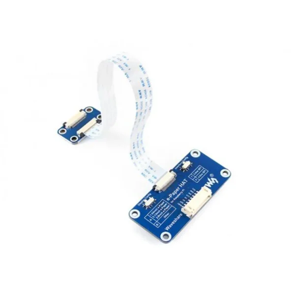 E-Paper Ink screen Driver Board HAT Raspberry Pi 40PIN GPIO Port 3-wire SPI/4-wire SPI For Raspberry Pi series/Jetson Nano
$15.70
E-Paper Ink screen Driver Board HAT Raspberry Pi 40PIN GPIO Port 3-wire SPI/4-wire SPI For Raspberry Pi series/Jetson Nano
$15.70
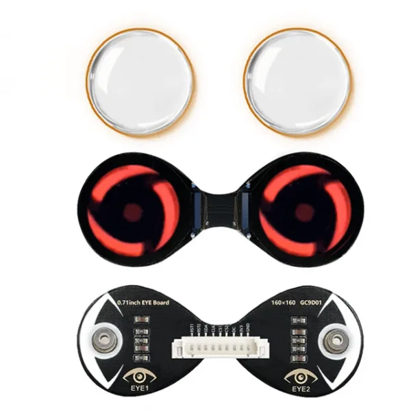 Double EYE 0.71 inch Round LCD Display Screen For Arduino Raspberry Pi ESP32 Pico STM32
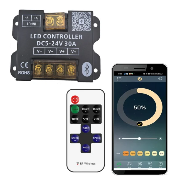 DC12-24V 30A 360W Mobile phone app Bluetooth connection LED Strip Controller dimmer With RF Touch Remote Use For LED Light
$5.90 – $6.30Price range: $5.90 through $6.30
DC12-24V 30A 360W Mobile phone app Bluetooth connection LED Strip Controller dimmer With RF Touch Remote Use For LED Light
$5.90 – $6.30Price range: $5.90 through $6.30
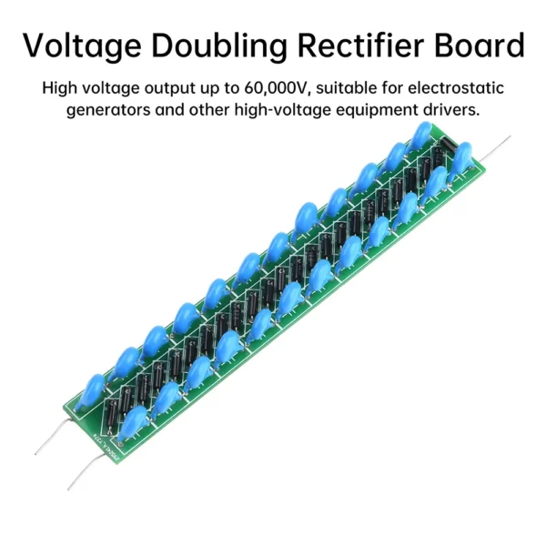 60KV Voltage Doubler Rectifying 24 Times Rectifier 60000V High Voltage Power Module for Generator Motor Electronic Kit
$12.90
60KV Voltage Doubler Rectifying 24 Times Rectifier 60000V High Voltage Power Module for Generator Motor Electronic Kit
$12.90
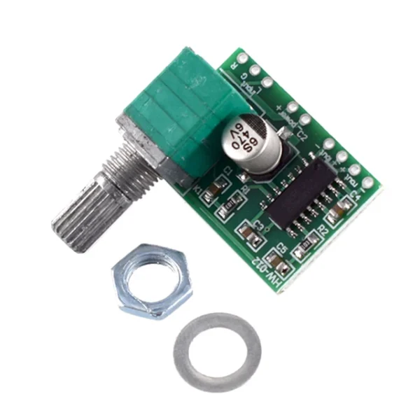 Mini PAM8403 DC 5V 2 Channel USB Digital Audio Amplifier Board Module 2 * 3W Volume Control with Potentionmeter
$2.30
Mini PAM8403 DC 5V 2 Channel USB Digital Audio Amplifier Board Module 2 * 3W Volume Control with Potentionmeter
$2.30