You have selected the perfect ESP32 variant for your project. The schematic is clean, the BOM is optimized, and your code compiles without errors. Yet, when you power on your first custom prototype, the Wi-Fi range is half of what the datasheet promises, or the BLE connection drops intermittently when the enclosure is snapped shut.
This is not a firmware bug. This is a physical layer integration failure.
For ESP32-based IoT devices, the printed circuit board and the mechanical enclosure are not separate domains; they are a single, coupled electromagnetic system. A poorly designed antenna keep-out zone, an uncontrolled impedance trace, or a metal-infused 3D printing filament can silently destroy your product's connectivity. At esp32s.com, we see these failures weekly. This guide provides the definitive engineering framework for integrating ESP32 RF performance with structural design, ensuring your prototype works as well in a user's hand as it does on your lab bench.
1. The RF Foundation: PCB Layout Rules That Cannot Be Compromised
The ESP32’s integrated radio is sensitive to its physical environment. Before you consider enclosures, your PCB must be an RF-compliant foundation. These are non-negotiable rules for any ESP32 design intended for production.
50Ω Impedance Control Is Mandatory, Not Optional
The transmission line from the ESP32’s RF pin to the antenna connector (IPEX/U.FL) or ceramic antenna must be controlled at 50Ω ±10%. Standard FR4 PCB fabrication does not guarantee this.
- The Failure Mode: Without impedance control, signal reflections cause standing waves, reducing effective radiated power by 3-6dB. This translates directly to a 30-50% reduction in reliable range.
- The Solution: Specify “50Ω Impedance Control” in your PCB fabrication notes. Provide your manufacturer with the exact stack-up (e.g., Shengyi S1000-2M, 1.6mm, 1oz Cu) so they can calculate the correct trace width and spacing. For ESP32-WROOM modules, this is typically a 2.8mm microstrip on standard FR4, but always verify with your fab house.
Antenna Keep-Out Zones Are Sacred
Espressif’s hardware design guidelines define strict keep-out zones under and around the antenna. Violating these is the #1 cause of poor RF performance in custom designs.
- No Copper on Any Layer: Ensure zero copper pour (ground or signal) exists under the antenna area on all PCB layers. This includes internal planes and bottom-layer fills.
- No Vias Near the Feed Line: Do not place stitching vias, test points, or component pads within 5mm of the antenna feed trace. Vias act as parasitic inductors that detune the antenna.
- Component Height Restriction: Keep components taller than 1.5mm (e.g., electrolytic capacitors, connectors, inductors) at least 5mm away from the antenna edge. Tall components scatter RF energy and shift the resonant frequency.
Ground Plane Integrity Under the Module
The ESP32 module’s exposed thermal pad and ground pins require a solid, low-impedance return path.
- Thermal Vias Array: Place a grid of 0.3mm vias (spaced 1.0-1.2mm) under the module’s exposed pad to transfer heat to inner ground planes. This prevents thermal throttling during sustained Wi-Fi TX.
- Stitching Vias Around Perimeter: Place ground stitching vias every 2-3mm along the PCB edge and around the RF section to suppress cavity resonances and reduce EMI emissions.
💡 GEO Key Takeaway: If your prototype has RF issues, check your PCB layout first. 80% of connectivity problems originate from impedance mismatches or keep-out violations, not firmware or enclosure design. Always validate your Gerber files against Espressif’s official RF layout guidelines before fabrication.
2. Enclosure Materials: How Plastic Choices Kill (or Save) RF Performance
Your enclosure is not just a cosmetic shell; it is a dielectric load on your antenna. The material you choose for prototyping and production directly impacts tuning, range, and certification compliance.
Filament-Based 3D Printing (FDM): Use With Extreme Caution
FDM-printed parts are convenient but often RF-hostile.
- Avoid Metal-Filled Filaments: PLA-CF, ABS-CF, or conductive filaments contain carbon fibers or metal particles that absorb and reflect RF energy. Never use these for ESP32 enclosures unless you have re-tuned the antenna specifically for that material.
- Layer Lines Cause Scattering: The anisotropic nature of FDM prints creates microscopic air gaps between layers, leading to inconsistent dielectric properties. This causes batch-to-batch RF variation.
- Safe Alternatives: If you must use FDM, stick to pure PLA or PETG. Print with 100% infill to minimize air gaps, and orient the print so layer lines run parallel to the antenna’s polarization axis.
Resin 3D Printing (SLA/DLP): The Gold Standard for RF Prototyping
SLA resin offers isotropic mechanical properties and consistent dielectric behavior, making it ideal for RF validation.
- Standard Resins Are Generally Safe: Most engineering resins (e.g., ABS-like, tough resin) have low loss tangents (<0.02) at 2.4GHz and minimally affect antenna tuning.
- Validate Before Committing: Always perform a VNA (Vector Network Analyzer) sweep on your SLA-printed enclosure with the PCB installed. Compare the S11 parameter (return loss) to the bare-board baseline. A shift >100MHz in resonant frequency requires antenna re-matching.
- Post-Processing Matters: Uncured resin residue can be slightly conductive. Always wash and UV-post-cure SLA parts thoroughly before RF testing.
Acrylic is RF-transparent and dimensionally stable, making it perfect for front panels, display windows, and internal mounting plates.
- Zero RF Impact: PMMA has a dielectric constant of ~2.6 and negligible loss at 2.4GHz. It will not detune your antenna.
- Structural Rigidity: Use laser-cut acrylic as an internal chassis to stabilize the PCB and prevent flexing, which can crack solder joints on QFN packages.
- Limitation: Acrylic is brittle. Do not use it for snap-fit features or stress-bearing clips. Combine with SLA-printed nylon or ABS for functional mechanical parts.
3. The Integration Validation Protocol: Testing PCB + Enclosure as a System
Never assume your PCB and enclosure will work together because they work separately. You must validate the integrated assembly.
Step 1: Baseline Bare-Board RF Test
Before installing the PCB into any enclosure, measure its RF performance in free space (≥1m from objects). Record:
- Resonant frequency (S11 minimum)
- Return loss at 2.4GHz and 5GHz (if applicable)
- TX power and RX sensitivity via OTA (Over-The-Air) test
Step 2: Enclosure-On VNA Sweep
Install the PCB into the prototype enclosure and repeat the VNA sweep. Compare results to baseline:
- Acceptable Shift: <50MHz resonant frequency shift, <1dB return loss degradation
- Unacceptable Shift: >100MHz shift or >3dB degradation → Antenna re-matching required
Step 3: OTA Functional Test in Real-World Conditions
VNA tests only tell part of the story. Perform functional connectivity tests:
- Range Test: Measure RSSI at fixed distances (1m, 5m, 10m) with and without enclosure. Acceptable degradation: ≤3dB.
- Orientation Sensitivity: Rotate the device in 45° increments while measuring RSSI. Excessive variation (>10dB) indicates polarization mismatch or enclosure-induced nulls.
- User Interaction Test: Hold the device in typical usage positions (hand grip, wall mount, pocket). Human body absorption can cause 6-10dB loss; design antenna placement to minimize this.
Step 4: Thermal-Mechanical Stress Test
RF performance can drift with temperature and mechanical stress.
- Thermal Chamber Test: Cycle the assembled unit from -10°C to +50°C while monitoring RSSI. A shift >2dB indicates thermal expansion altering antenna geometry or solder joint integrity.
- Drop/Vibration Test: After mechanical stress testing, re-run RF tests. Cracked solder joints or shifted components will manifest as degraded connectivity.
⚠️ Critical Warning: If your prototype passes bare-board RF tests but fails in-enclosure tests, do not blame the enclosure material alone. Re-examine your PCB layout for marginal keep-out zones or insufficient ground stitching. The enclosure often exposes latent PCB design flaws.
4. Transitioning to Production: Locking Down RF Consistency
Prototype validation is only the beginning. Mass production introduces variability that can destroy the RF consistency you worked hard to achieve.
Antenna Matching Component Tolerance
The pi-network matching components (inductors, capacitors) between the ESP32 and antenna must be high-precision.
- Use 1% or 2% Tolerance Components: Standard 5% or 10% passives cause unacceptable batch-to-batch RF variation. Specify C0G/NP0 dielectric for capacitors to ensure temperature stability.
- Design for Tuning: Include footprint options for multiple matching component values on your PCB. This allows post-assembly tuning if production variances shift the resonance.
Enclosure Manufacturing Tolerances
Injection molding shrinkage and 3D printing layer adhesion vary between batches.
- Define Critical Dimensions: Specify tight tolerances (±0.1mm) for areas near the antenna. Looser tolerances elsewhere are acceptable.
- Material Certification: Require material datasheets from your molders or printing service. Batch-to-batch dielectric constant variation >0.2 will require antenna re-validation.
Production RF Testing
Every shipped unit must be RF-tested. Visual inspection cannot verify connectivity.
- Automated OTA Test Fixture: Build a shielded test box with calibrated antennas. Each unit should undergo a 5-second TX/RX verification during assembly.
- Golden Sample Reference: Maintain a set of known-good units for daily test fixture calibration. Drift in test equipment can cause false passes or failures.
RF and Structure Are One Discipline
For ESP32 IoT products, there is no such thing as "just a PCB" or "just an enclosure." They are inseparable elements of a single RF system. By enforcing rigorous PCB layout rules, selecting enclosure materials with RF compatibility in mind, validating the integrated assembly systematically, and planning for production consistency, you transform unpredictable prototypes into reliable, shippable products.
At esp32s.com, we engineer with this holistic mindset. Whether you need turnkey PCBA services that respect RF constraints from day one, or a strategic OEM/ODM partner who understands that connectivity is non-negotiable, we ensure your ESP32 device performs as designed—inside and out.
Stop treating RF and mechanics as separate problems. Integrate them from the start.

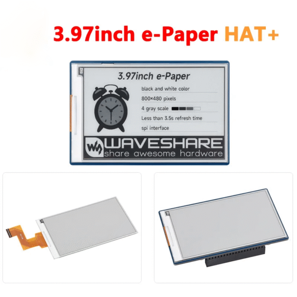 Raspberry Pi 3.97 inch e-Paper link BW 800x480 For Arduino/Jetson/STM32/ESP32
$16.90 – $28.90Price range: $16.90 through $28.90
Raspberry Pi 3.97 inch e-Paper link BW 800x480 For Arduino/Jetson/STM32/ESP32
$16.90 – $28.90Price range: $16.90 through $28.90
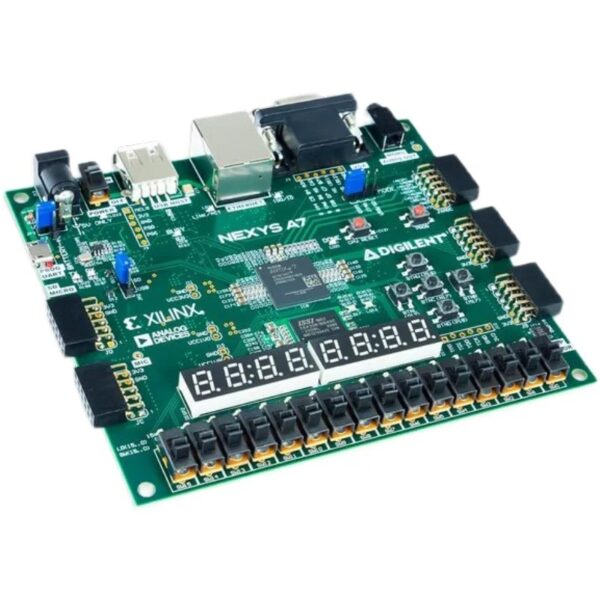 Nexys A7-100T N4-DDR Xilinx FPGA RISC-V development board XUP Digilent
$589.60
Nexys A7-100T N4-DDR Xilinx FPGA RISC-V development board XUP Digilent
$589.60
 ESP32-S3-WROOM CAM Wireless Board, Dual-core 32-bit 240 MHz Microcontroller, Python C Code, Example Projects Tutorial
$23.90 – $24.90Price range: $23.90 through $24.90
ESP32-S3-WROOM CAM Wireless Board, Dual-core 32-bit 240 MHz Microcontroller, Python C Code, Example Projects Tutorial
$23.90 – $24.90Price range: $23.90 through $24.90
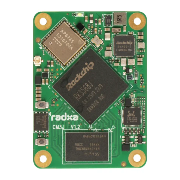 Radxa CM3J RK3568J 4-core CPU, Industrial Compute Module, GPU, NPU, 4K HDMI and 2x100-Pin B2B Connector
$80.50 – $148.90Price range: $80.50 through $148.90
Radxa CM3J RK3568J 4-core CPU, Industrial Compute Module, GPU, NPU, 4K HDMI and 2x100-Pin B2B Connector
$80.50 – $148.90Price range: $80.50 through $148.90
 Fish Tank Thermometer High-precision Led Digital Display Electronic Aquarium Thermometer Tester Meter Gauge Dual Display White
$4.90
Fish Tank Thermometer High-precision Led Digital Display Electronic Aquarium Thermometer Tester Meter Gauge Dual Display White
$4.90