Passing Design Rule Checks (DRC) and Electrical Rule Checks (ERC) only confirms logical connectivity. It does not validate physical manufacturability. When a board with a clean schematic consistently fails during Surface Mount Technology (SMT) assembly—exhibiting tombstoning, BGA voiding, or cold joints—the root cause is almost always embedded in the physical layout.
Solder paste is a thixotropic fluid, and reflow is a thermodynamic event. If the copper layout creates thermal imbalances or capillary traps, no adjustment to the reflow profile or stencil thickness will compensate for the fundamental design flaw.
Thermal Asymmetry and Component Tombstoning
Tombstoning on small chip components (0402, 0201) is rarely caused by pick-and-place machine inaccuracy. It is a direct result of thermal asymmetry baked into the copper layout.
During reflow, both ends of a component must reach the solder's liquidus temperature simultaneously. If one pad is connected to a massive, unbroken ground pour and the other is connected to a narrow signal trace, the ground pad acts as a heat sink. It dissipates heat away from the joint much faster than the trace pad.
As the temperature rises, the solder on the trace pad melts first. The surface tension of that single molten joint pulls the component upright, standing it on its end before the second pad can melt.
The Layout Correction: This cannot be fixed by tweaking the reflow oven profile. The layout must be modified.
- Apply thermal reliefs (cross-hatched connections) to pads tied to large copper planes to restrict heat dissipation.
- If a solid connection is required for high-current applications, ensure the copper distribution is perfectly symmetrical on both pads.
- Route fine-pitch and small chip components away from the immediate edges of large thermal masses.
Capillary Action and Via-in-Pad Defects
Placing an unplugged via directly inside an SMD pad is a common routing shortcut that leads to predictable soldering defects.
During the reflow phase, molten solder behaves as a fluid. If an open via exists on the pad, capillary action will wick the solder down into the hole. This starves the joint of necessary solder volume. On fine-pitch components, this causes bridging. On Ball Grid Arrays (BGAs), it leads to massive voiding or the "head-in-pillow" defect, where the solder ball and the paste fail to fully coalesce due to flux exhaustion and volume loss.
The Layout Correction: If a via must be placed on a pad for thermal dissipation or routing density, it cannot be left open.
- Specify Via-In-Pad Plated Over (VIPPO), where the via is resin-filled and capped with copper during fabrication.
- If VIPPO exceeds the project budget, the via must be tightly plugged with solder mask to block capillary action, though this is less reliable than resin filling.
- Never route a via directly under a BGA ball without explicit confirmation from the PCB fabricator regarding their via-plugging capabilities.
Hydrodynamic Shadows in Wave Soldering
For mixed-technology boards combining SMT and Through-Hole (THT) components, the physical layout of component heights dictates the success of the wave soldering process.
If a tall electrolytic capacitor or a large connector is placed immediately upstream (in the direction of the solder wave flow) of a smaller component, the tall component creates a physical hydrodynamic shadow. The molten wave flows around the tall component, creating a turbulent wake that prevents the solder from properly wetting the pads in the shadow zone. This results in cold solder joints or non-wetting defects.
The Layout Correction:
- Orient the board layout so that the wave flows from the shortest components to the tallest.
- Maintain a strict clearance zone (typically 3mm to 5mm) downstream of tall components in the direction of the wave flow.
- If board space is constrained, the small components in the shadow zone should be moved to the opposite side of the board and processed via reflow, bypassing the wave soldering step entirely.
Correcting Layout-Driven Assembly Failures
Adjusting solder paste viscosity or changing stencil thickness cannot fix a board with fundamental thermal or capillary flaws. The defect is locked into the Gerber files. If a hardware team is experiencing recurring SMT yield issues, the root cause requires intervention at the layout stage.
Designing for manufacturing demands a shift from pure schematic capture to understanding stack-up impedance, thermal relief geometry, and SMT kinematics. If current designs are suffering from assembly failures, our professional PCB Layout and Design services provide the necessary engineering oversight. We optimize thermal management, enforce strict DFM clearances, and structure via arrays to eliminate voiding before the files reach the fabrication house.
Validating these layout corrections requires physical testing. Spinning a full-sized, multi-layer prototype solely to test a routing tweak is an inefficient use of resources. To remove the financial friction of physical validation, we maintain a strategic prototyping initiative: $2 for 5 pieces for custom PCB under 50mm x 50mm.
Hardware engineers can use this program to fabricate dedicated DFM test coupons. This allows for empirical verification of new thermal relief patterns, via-in-pad structures, and fine-pitch pad geometries at a fraction of the cost of a standard prototype. Once the layout is proven, the design can seamlessly transition to full-sized builds through our comprehensive PCB and PCBA production service.
For the fine-pitch components discussed above, precise solder paste deposition is equally critical. We supply high-precision SMT stencils with optimized aperture reductions, such as step-down or nano-coated options, tailored specifically to the layout's pad geometry to ensure perfect paste volume.
When the layout is validated and ready for high-volume manufacturing, initiating an OEM/ODM bulk manufacturing inquiry allows our process engineering team to lock these validated DFM rules into the mass-production control plan. For direct technical discussions regarding specific layout challenges or stack-up requirements, please contact us to speak with our engineering team.
Frequently Asked Questions
Q: Can adjusting the reflow profile fix tombstoning caused by asymmetric copper pours?
A: No. Adjusting the reflow profile might temporarily mask the symptom, but it will likely introduce other defects, such as head-in-pillow on BGAs or insufficient wetting on larger joints. Tombstoning driven by thermal asymmetry is a physical imbalance that must be corrected in the PCB layout using thermal reliefs or symmetrical copper distribution.
Q: Why does a BGA show high voiding on X-ray even with a new stencil?
A: High voiding in BGAs is frequently caused by outgassing from the PCB substrate or solder mask, which gets trapped under the component during reflow. It is also commonly caused by open vias in the BGA pads that allow flux and gases to expand into the joint. The layout must utilize resin-filled and capped vias (VIPPO) under BGA pads to prevent this.
Q: What is the minimum clearance required between a tall connector and the next component for wave soldering?
A: As a general rule, a minimum clearance of 3mm to 5mm downstream (in the direction of the solder wave flow) is required from any tall component. Smaller clearances create a shadow effect, preventing the solder wave from properly wetting the pads of the component behind it.
Q: Is a DFM check performed before fabrication?
A: Yes. Every order placed through our PCB Layout and Design services and PCB and PCBA production undergoes a rigorous engineering DFM review. We check for thermal imbalances, via-in-pad issues, acid traps, insufficient annular rings, and SMT clearance violations, providing a detailed report before manufacturing begins.

 Excellent Esp32-Aduio-Kit Wifi+ Bluetooth Module Esp32 Serial To Wifi / Esp32-Aduio-Kit Audio Development Board With Esp32-A1S
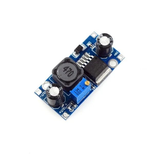 LM2596S DC-DC 3A 92% Step-down Power Supply Module Adjustable Step-down module 3.2V-35V To 1.25V-30V Voltage Regulator
$2.50
LM2596S DC-DC 3A 92% Step-down Power Supply Module Adjustable Step-down module 3.2V-35V To 1.25V-30V Voltage Regulator
$2.50
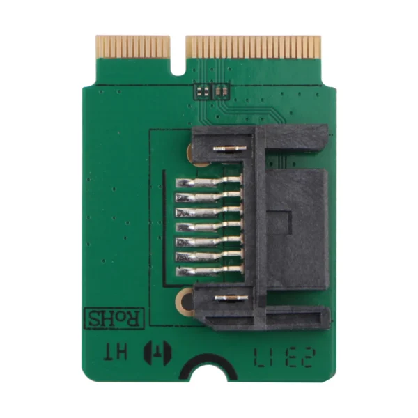 Radxa M.2 E Key to SATA Breakout Board for M.2 E Key interface support SATA
$5.90
Radxa M.2 E Key to SATA Breakout Board for M.2 E Key interface support SATA
$5.90
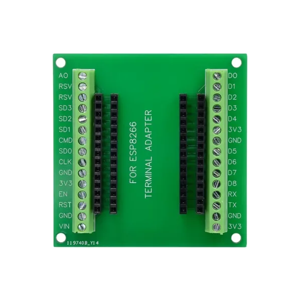 ESP32 ESP8266 Breakout Board GPIO 1 into 2 Compatible with 38 Pins ESP32S ESP32 Development Board 2.4 GHz Dual Core for Arduino
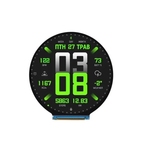 ESP32-S3 2.8inch Round Display Development Board, 480×480, 32-bit LX7 Dual-core Processor, Options For Touch Function
$32.90 – $37.90Price range: $32.90 through $37.90
ESP32-S3 2.8inch Round Display Development Board, 480×480, 32-bit LX7 Dual-core Processor, Options For Touch Function
$32.90 – $37.90Price range: $32.90 through $37.90