You’ve spent months optimizing your firmware. You’ve carefully configured the ESP32-S3 to enter Deep Sleep, meticulously calculating that your device should run for two years on a single CR2032 coin cell or a small Li-Po battery.
You send your Gerber files off, receive the assembled prototype, flash the code, and… the battery dies in three days.
What went wrong? Did Espressif change the silicon? Is your code broken?
In 90% of these cases, the culprit isn’t the code or the chip. The culprit is the PCBA manufacturing process.
At esp32s.com, we specialize in manufacturing high-reliability, low-power IoT devices. We’ve seen countless designs fail in the field not because of bad engineering, but because of invisible manufacturing defects that cause parasitic leakage currents.
In this deep-dive guide, we will expose the hidden PCBA killers of battery life and reveal the exact manufacturing protocols you must demand from your assembly partner to ensure your ESP32 device achieves its theoretical battery life.
Killer #1: Ionic Contamination & Surface Leakage
The Pain Point: Your ESP32 draws 5µA in Deep Sleep on a dry Tuesday, but 500µA on a humid Thursday. The Technical Reality: During the SMT reflow process, solder paste leaves behind flux residues. If "No-Clean" flux is used but not properly activated, or if water-soluble flux is inadequately cleaned, it leaves behind ionic contaminants (salts and acids) on the PCB surface. In a dry environment, these residues are harmless. But in the real world (with humidity, dust, and temperature swings), these ions absorb moisture and create microscopic conductive paths between high-impedance nodes (like the ESP32’s RTC_GPIO pins or the feedback loop of your LDO regulator). This causes surface leakage current, completely destroying your low-power budget.
The PCBA Fix:
- Strict Cleaning Protocols: For ultra-low-power designs, do not rely on standard "No-Clean" processes. Demand that your PCBA partner performs a rigorous aqueous or solvent cleaning process post-reflow to remove all ionic residues.
- Ionography Testing: A professional manufacturer will periodically test batch panels using an Ionograph to measure surface contamination levels (measured in µg/NaCl eq/in²), ensuring they are well below the IPC-standard threshold of <1.55 µg/in².
Killer #2: MLCC Micro-Cracks from Thermal & Mechanical Stress
The Pain Point: The device works perfectly in the lab, but fails intermittently in the field, or the battery drains rapidly after a few months of vibration/temperature cycling. The Technical Reality: Multi-Layer Ceramic Capacitors (MLCCs) are the workhorses of your decoupling circuits. However, they are highly brittle. If the reflow oven temperature profile is too aggressive (causing thermal shock), or if the PCB depaneling (routing/V-scoring) process exerts mechanical bending stress on the board, microscopic cracks can form inside the ceramic layers. These micro-cracks might not cause an immediate short circuit. Instead, over time, moisture and contaminants penetrate the cracks, leading to internal leakage currents or eventual catastrophic failure.
The PCBA Fix:
- Optimized Reflow Profiling: The PCBA engineer must tailor the thermal profile specifically for the board’s thermal mass, ensuring a gentle ramp-up rate (typically < 2°C/second) to prevent thermal shock to the MLCCs.
- Stress-Relief Depaneling: Avoid simple V-score breaking for boards with heavy components or tight tolerances. Use CNC routing or laser depaneling which eliminates mechanical bending stress entirely, preserving the integrity of the capacitors.
Killer #3: Poor Wetting on Battery Connectors & High-Current Paths
The Pain Point: The ESP32 randomly reboots exactly when the Wi-Fi radio transmits (which requires a sudden spike of ~500mA). The Technical Reality: The Wi-Fi transmission spike is massive. If the solder joints on the battery connector, or the vias connecting your power planes, have poor wetting (insufficient solder fillet) or cold solder joints, they introduce parasitic resistance. When the ESP32 pulls 500mA, this resistance causes a sudden voltage drop (V = IR). If the voltage at the ESP32’s VDD pin dips below its brown-out detector threshold, the chip resets.
The PCBA Fix:
- Automated Solder Paste Inspection (SPI): Before components are placed, an SPI machine must verify the exact volume and height of the solder paste on every pad. This prevents "starved" joints before they even happen.
- Selective Wave Soldering or Precision Hand Soldering: For through-hole battery connectors or heavy power terminals, reflow soldering often isn't enough due to thermal mass differences. Using selective soldering or highly trained manual soldering with strict temperature-controlled irons ensures 100% wetting and zero parasitic resistance.
Killer #4: The Double-Edged Sword of Conformal Coating
The Pain Point: To protect against humidity, you apply a conformal coating (三防漆), but suddenly your Wi-Fi range drops by 50%, or your capacitive touch sensors stop working. The Technical Reality: Conformal coatings (like Acrylic, Silicone, or Polyurethane) are essential for outdoor or harsh-environment IoT devices. However, they have a dielectric constant (Dk) that is different from air. If applied over the ESP32’s PCB trace antenna or chip antenna, it detunes the antenna, shifting the resonant frequency and destroying your RF range. Furthermore, if coating seeps into the moving parts of a switch or connector, it causes mechanical failure.
The PCBA Fix:
- Precision Masking or Selective Coating: Never use manual spray cans for production. Use automated selective conformal coating machines with UV-traceable fluids. This allows the machine to precisely apply the coating only where needed, leaving the RF antenna keep-out zones, connectors, and test points completely bare.
- RF Re-Tuning: If coating is absolutely required near the antenna area, the PCB antenna must be re-tuned (adjusting the matching network Pi-circuit) after the coating is applied to compensate for the dielectric shift.
The esp32s.com Advantage: Micro-Amp Testing & Reliability First
Understanding these pitfalls is one thing; having the factory equipment and expertise to prevent them is another.
When you partner with esp32s.com for your low-power IoT PCBA, we don't just stuff components. We engineer for reliability:
- Deep Sleep Current Testing: We can set up a custom test fixture to measure the actual Deep Sleep current of every assembled board before it ships. If a board draws 50µA instead of the expected 5µA, we catch it and rework it before it reaches your hands.
- Advanced Cleaning & Coating: We offer professional aqueous cleaning and automated selective conformal coating services, ensuring your boards survive the real world without sacrificing battery life or RF performance.
- X-Ray & 3D AOI: As mentioned in our previous guides, we use X-ray to inspect the hidden pins of the ESP32 module and 3D AOI to verify solder paste volume, eliminating micro-cracks and cold joints.
Is Your PCBA Partner Sabotaging Your Battery Life?
If you are building a battery-powered ESP32 device, you cannot afford to treat PCB assembly as a "commodity" service. The cheapest quote often comes from a factory that skips cleaning, uses aggressive depaneling, and lacks micro-amp testing capabilities. The cost of a field failure or a battery recall will dwarf your initial savings.
Don't let invisible manufacturing flaws kill your product's reputation. Partner with a team that understands the physics of low-power IoT.
Frequently Asked Questions (FAQ)
Q: How do you test for leakage current on assembled low-power boards?
A: For low-power prototypes and production runs, we can integrate a "Deep Sleep Current Test" into our functional testing (FCT) phase. We power the board via a precision source-measure unit (SMU), trigger the firmware's sleep mode, and verify that the current draw matches your design specification (e.g., < 10µA). Boards failing this threshold are flagged for inspection and rework.
Q: Do you offer conformal coating services, and how do you protect the ESP32 antenna?
A: Yes, we offer automated selective conformal coating (using acrylic, silicone, or polyurethane materials). We use UV-traceable coatings and precise masking programs to ensure the RF antenna keep-out zone, connectors, and test points remain completely uncoated, preserving your Wi-Fi/Bluetooth range and mechanical functionality.
Q: How do you prevent MLCC micro-cracks during manufacturing?
A: We prevent thermal stress by using optimized, multi-zone reflow oven profiles with controlled ramp-up rates. To prevent mechanical stress, we avoid manual V-score breaking for sensitive boards, preferring CNC routing or laser depaneling which eliminates bending stress entirely.
Q: Can you help me choose the right battery connector or power management IC for my ESP32 design?
A: Absolutely. Our engineering team provides free DFM and Design for Cost (DFC) reviews. If your current BOM includes components known for high quiescent current or poor solderability, we will suggest drop-in alternatives that optimize both battery life and manufacturing yield.

 Radxa ZERO 3W/3E Series 5519A Heatsink
$5.90
Radxa ZERO 3W/3E Series 5519A Heatsink
$5.90
 GUVA-S12SD Light Sensor DIY Kit 240nm-370nm UV Sunlight Intensity Sensor Light Intensity Detection Sensor Board for Arduino
$4.90
GUVA-S12SD Light Sensor DIY Kit 240nm-370nm UV Sunlight Intensity Sensor Light Intensity Detection Sensor Board for Arduino
$4.90
 SenseCAP S700-B 7-in-1 Compact Weather Station with Solar Radiation Shield,Temp,Humidity,Rain,Wind,Pressure,Ultrasonic& Optical
$1,000.00
SenseCAP S700-B 7-in-1 Compact Weather Station with Solar Radiation Shield,Temp,Humidity,Rain,Wind,Pressure,Ultrasonic& Optical
$1,000.00
 OV9281 USB Industrial Camera Module – Global Shutter, Monochrome, 120fps High-Speed, Driver-Free, Adjustable Field of View
$30.90
OV9281 USB Industrial Camera Module – Global Shutter, Monochrome, 120fps High-Speed, Driver-Free, Adjustable Field of View
$30.90
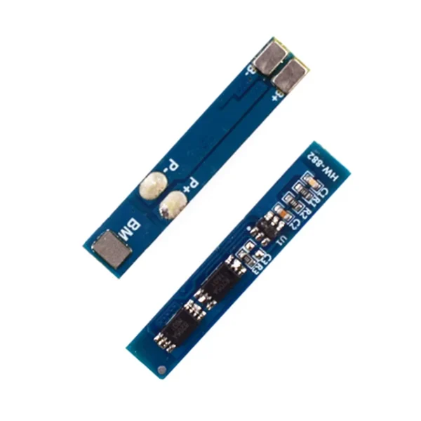 5PCS 2S 3A Li-ion Lithium Battery 7.4v 8.4V 18650 Charger Protection Board bms pcm for li-ion lipo battery cell pack
$7.90
5PCS 2S 3A Li-ion Lithium Battery 7.4v 8.4V 18650 Charger Protection Board bms pcm for li-ion lipo battery cell pack
$7.90