When hardware engineers and procurement managers evaluate a PCBA (Printed Circuit Board Assembly) partner, they don't just want a list of machines on the factory floor. They want to know how your process control guarantees yield, how you manage the transition from prototype to mass production, and whether your quality standards align with IPC-A-610.
SMT (Surface Mount Technology) and DIP (Dual In-line Package) processes are highly complex. A minor deviation in solder paste volume or reflow temperature can lead to catastrophic field failures. This guide cuts through generic factory brochures. We will break down the actual PCBA manufacturing process, highlight the critical process control parameters that separate top-tier manufacturers from the rest, and explain how to secure a reliable turnkey assembly partner.
Phase 1: SMT Assembly & Process Control (The 99% Yield Factor)
SMT accounts for the vast majority of modern PCBA work. However, simply running boards through a pick-and-place machine is not enough. The real value lies in closed-loop process control.
1. Solder Paste Printing & SPI Closed-Loop
The solder paste printing step dictates over 60% of all soldering defects. We use laser-cut stainless steel stencils (typically 0.08mm–0.15mm thick) and lead-free SAC305 (Sn96.5/Ag3.0/Cu0.5) paste.
- The Game Changer (SPI): After printing, the board immediately passes through a 3D Solder Paste Inspection (SPI) machine. SPI doesn't just flag defects; it measures volume, height, and area with ±2μm accuracy. Crucially, this data is fed back to the printer in real-time to adjust blade pressure and speed, creating a closed-loop SPC (Statistical Process Control) system that prevents defects before they happen.
2. High-Speed & Fine-Pitch Placement
Modern SMT lines utilize a combination of high-speed chip shooters (≥40,000 CPH for 0201/resistors) and multi-function placers (for QFNs, BGAs, and connectors).
- Process Control: Nozzle selection and Z-axis placement pressure are strictly calibrated. Placing a BGA with excessive force will cause solder paste slump and bridging; too little force will result in tombstoning or open joints during reflow.
3. Reflow Soldering & Thermal Profiling
Reflow is where the metallurgical bond is formed. For lead-free SAC305, the thermal profile is strictly monitored across 8 to 12 temperature zones.
- Critical Parameters: The peak temperature is strictly maintained between 240°C and 250°C (never exceeding 260°C to prevent component damage). The Time Above Liquidus (TAL) is tightly controlled between 40 and 90 seconds. If the TAL is too long, brittle Intermetallic Compounds (IMC) overgrow, leading to weak solder joints.
4. AOI & X-Ray Inspection
Post-reflow, boards pass through Automated Optical Inspection (AOI). Modern AOI utilizes AI deep-learning algorithms to distinguish between true defects (bridging, tombstoning, missing parts) and acceptable cosmetic variations, reducing false calls to <0.05%.
- Hidden Joints: For BGAs, CSPs, and QFNs, AOI is blind. We mandate X-Ray inspection to verify solder joint integrity, ensuring voiding rates remain strictly below the IPC-7095 standard limit of 25%.
Phase 2: Through-Hole (DIP) & Selective Soldering
For boards requiring the mechanical robustness of Through-Hole Technology (THT), the assembly process shifts to DIP and wave soldering.
1. Standard Wave Soldering
After manual or auto-insertion, the board passes through a wave soldering machine. The process includes flux spraying, preheating (90°C–130°C to activate the flux and prevent thermal shock), and contact with the molten solder wave (250°C–260°C for lead-free).
- Common Pitfalls: Poor through-hole fill (insufficient wetting) and solder bridging are common if the conveyor speed (typically 0.8–1.5m/min) and contact depth are not perfectly balanced.
2. Selective Wave Soldering (The High-Mix Solution)
For complex PCBA boards mixing dense SMT components with scattered THT parts, traditional wave soldering causes severe thermal stress to the SMT components. Selective soldering solves this by using a programmable mini-solder nozzle to target only specific through-hole pads. This minimizes thermal shock, reduces flux usage, and is ideal for high-reliability automotive and industrial boards.
Phase 3: Conformal Coating & Environmental Protection
For electronics operating in harsh environments (automotive, outdoor IoT, medical), conformal coating is non-negotiable. Choosing the wrong material will lead to premature failure. Here is the engineering reality of coating selection:
Process Note: We utilize automated selective coating machines with UV tracing to ensure precise application (typically 25μm–75μm thickness) while masking connectors and test points, eliminating the human error associated with manual brushing.
Phase 4: Testing & Quality Assurance (The Final Gate)
A PCBA is only as good as its test coverage. We implement a multi-tiered testing strategy based on IPC-A-610 and IPC-J-STD-001 standards:
- ICT (In-Circuit Test): Uses a bed-of-nails fixture to verify individual component values and detect opens/shorts at the component level. Ideal for high-volume production.
- FCT (Functional Circuit Test): Custom test jigs power up the board and simulate real-world operating conditions, verifying firmware, power delivery, and signal integrity.
- Burn-In Testing: For mission-critical applications, boards are subjected to elevated temperatures and continuous power for 24 to 72 hours to weed out early-life infant mortality failures.
The Hidden Bottleneck: Transitioning from Prototype to Mass Production
The most dangerous phase in hardware development is the transition from a 10-piece prototype to a 5,000-unit production run. Prototypes are often built with manual workarounds, but mass production requires strict adherence to the thermal profiles and stencil designs mentioned above. A minor DFM (Design for Manufacturability) flaw ignored during prototyping will become a massive yield killer at scale.
To bridge this gap, you must partner with a facility that handles the entire lifecycle. Utilizing our turnkey PCB prototype and assembly manufacturing service ensures that the DFM feedback and process parameters validated during your first 5 prototype boards are directly locked into the mass-production SMT programming. This eliminates the "re-engineering shock" and ensures a seamless transition to volume.
Scaling Up: OEM/ODM Bulk Manufacturing Strategy
Once your design is validated, the focus shifts to supply chain resilience, component allocation, and cost optimization. Sourcing bare boards, components, and assembly from three different vendors is a recipe for logistical nightmares and accountability gaps.
If you are preparing to scale your product line, initiating an OEM/ODM bulk manufacturing inquiry early in your design cycle allows our engineering team to align your BOM with the most cost-effective panelization strategies and secure long-lead component allocation. Single-point accountability drastically reduces lead times and eliminates the "blame game" between suppliers.
The Startup Advantage: Rapid Prototyping Without Financial Risk
We understand that for hardware startups and independent developers, the cost of multiple prototype iterations to validate mechanical fit and basic circuit functionality can drain an R&D budget.
This is a strategic engineering tool that allows you to:
- Validate your schematic and basic layout with real, production-grade physical boards.
- Test different component footprints or thermal via patterns without financial penalty.
- Accelerate your R&D cycle by ordering multiple design variants simultaneously.
Frequently Asked Questions (FAQ)
Q: What is the acceptable voiding rate for BGA solder joints?
A: According to IPC-7095 standards, the maximum acceptable voiding area for standard applications is 25%. However, for high-reliability automotive or medical products, our process control routinely achieves voiding rates of <10% through optimized reflow profiles and vacuum reflow options.
Q: How do you prevent tombstoning on ultra-small components like 0201?
A: Tombstoning is primarily caused by uneven heating or pad design asymmetry. We prevent this by enforcing strict IPC-7351 land patterns, ensuring symmetrical thermal relief, and utilizing SPI to guarantee exact solder paste volume on both pads.
Q: Can you handle mixed-technology boards with both SMT and complex THT components?
A: Yes. We utilize selective wave soldering for mixed-technology boards. This allows us to solder THT components precisely without exposing the already-assembled, temperature-sensitive SMT components to the thermal shock of a traditional wave soldering process.
Q: What IPC standards does your PCBA manufacturing comply with?
A: Our manufacturing and inspection processes are strictly aligned with IPC-A-610 (Acceptability of Electronic Assemblies) Class 2 and Class 3 standards, and IPC-J-STD-001 (Requirements for Soldered Electrical and Electronic Assemblies).
Stop Gambling with Your PCBA Manufacturing
High-quality PCBA manufacturing is not about having the most machines; it is about rigorous process control, strict adherence to IPC standards, and a seamless transition from prototype to mass production.
Whether you are utilizing our $2 for 5 pieces (under 50x50mm) offer to validate your initial layout, or you are ready to scale a complex, mixed-technology design into high-volume production, our engineering team is prepared to provide the actionable DFM feedback and precision manufacturing your project demands.
Ready to build with confidence?
Reach out to our engineering team today for a comprehensive DFM review and a precise manufacturing quote. Let's engineer a product that performs flawlessly in the field.

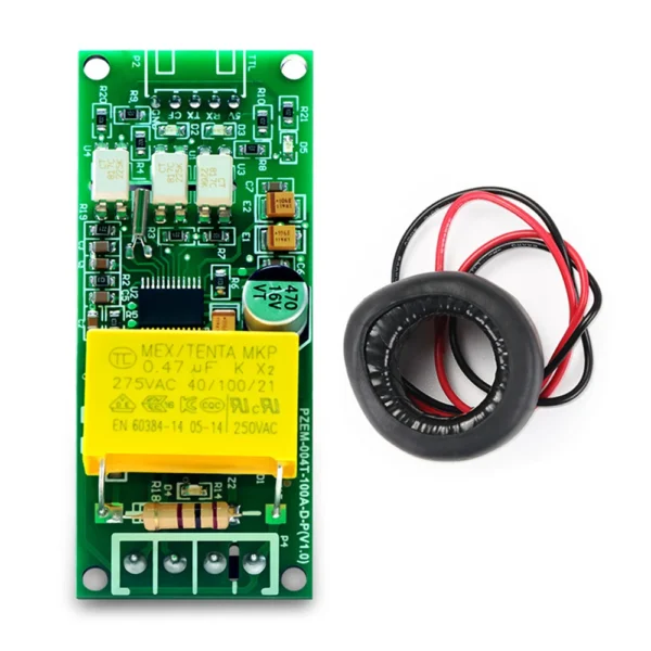 PZEM-004T 100A AC 80-260V Digital Voltmeter Ammeter Wattmeter Digital Multifunctional Test Pulse Communication TTL Serial Module
$5.20 – $7.80Price range: $5.20 through $7.80
PZEM-004T 100A AC 80-260V Digital Voltmeter Ammeter Wattmeter Digital Multifunctional Test Pulse Communication TTL Serial Module
$5.20 – $7.80Price range: $5.20 through $7.80
 ESP32-S3 WROOM N16R8 Development Board 2.4G Wifi BT Camera Module OV2640 OV5640 16MB FLASH 8MB PSRAM ESP32 S3 N16R8 CAM
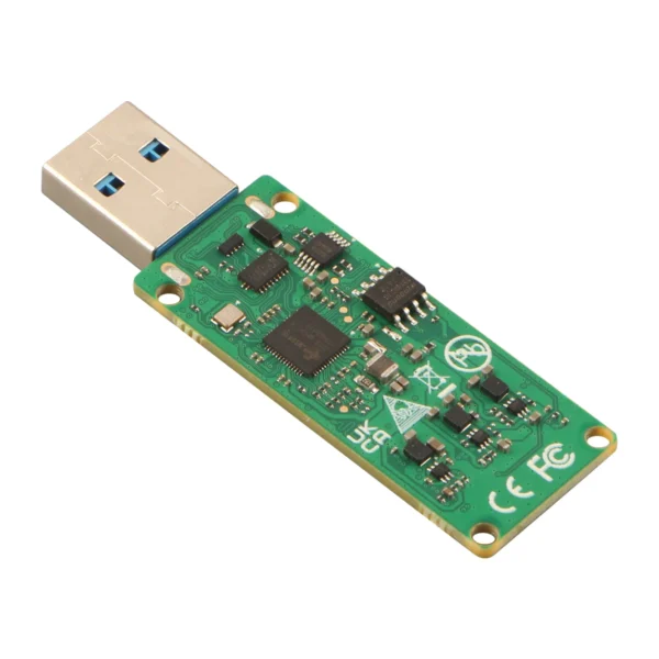 Radxa UFS/eMMC Module Reader Designed for Radxa SBCs
$20.90
Radxa UFS/eMMC Module Reader Designed for Radxa SBCs
$20.90
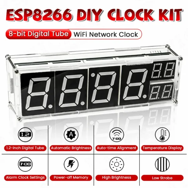 DIY Kit Electronic Network Clock WiFi ESP8266 Module 8-bit Digital Tube Display Time Temperature Alarm Soldering Practice Kit
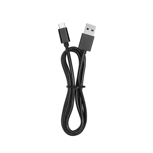 Radxa AC002C USB-A to USB-C Charging Data Cable
$4.90
Radxa AC002C USB-A to USB-C Charging Data Cable
$4.90