When components fail on the PCBA production line, the root cause is often obvious. However, the most costly ESD (Electrostatic Discharge) events are the ones that go unnoticed. A partial discharge can degrade a semiconductor’s internal oxide layer or P-N junction without causing immediate catastrophic failure. The component passes In-Circuit Test (ICT) and Functional Circuit Test (FCT), ships to the customer, and fails prematurely in the field.
Eliminating these latent defects requires more than just issuing wrist straps. It demands a rigorously audited control plan aligned with ANSI/ESD S20.20. This document outlines the specific engineering parameters, zoning protocols, and continuous monitoring procedures required to maintain a compliant Electrostatic Discharge Protected Area (EPA) in high-volume PCBA manufacturing.
EPA Zoning and Environmental Parameters
Static charge generation accelerates exponentially when ambient relative humidity drops. Control begins with strict physical demarcation and climate management.
Level 1 EPA (High Sensitivity): Designated for handling components with a Human Body Model (HBM) sensitivity of <2000V (e.g., CMOS ICs, MOSFETs, BGAs). This includes SMT placement lines, BGA rework stations, and precision testing areas.
- Demarcation: Solid yellow floor lines (50mm width). Mandatory continuous wrist strap usage.
- Climate Control: Maintained at 20°C–25°C and 45%–60% RH. Automated humidification/dehumidification systems trigger if parameters deviate by >5%.
Level 2 EPA (General Sensitivity): Designated for components with HBM sensitivity between 2000V and 4000V (e.g., standard passives). Includes DIP assembly and post-wave soldering areas.
- Demarcation: Dashed yellow floor lines. Mandatory ESD-safe footwear and garments.
Ionization for Insulators: Grounding cannot neutralize charges on insulating materials like plastic component reels or bare PCB substrates. In Level 1 EPAs, overhead ionizing air blowers are positioned directly above SMT feeders and unpacking stations. Performance is verified weekly using a charged plate monitor, requiring an ion balance of ±50V (at 30cm) and a decay time of ≤10 seconds (from ±1000V to ±100V).
Personnel and Equipment Grounding Integrity
The grounding infrastructure is the baseline of EPA compliance. A grounded operator is ineffective if the workbench or tooling is floating at a high potential.
- Wrist Strap Protocol: All personnel handling ESD-sensitive devices must wear wired wrist straps incorporating a 1MΩ series safety resistor. This resistor limits discharge current to safe levels (<0.5mA), protecting the operator from electrical shock while safely bleeding off static charges. Testing is mandatory at the start of every shift.
- Facility and Workbench Grounding: The main ESD ground must be independent of the electrical power ground to prevent noise coupling, maintaining a total resistance of ≤4Ω. ESD matting (surface resistance 10⁶–10⁹ Ω) is connected to this ground via 1MΩ safety resistors and verified weekly.
- Soldering and Rework Tools: A frequent point of failure. ESD-safe soldering irons must maintain a tip-to-ground resistance of ≤2Ω and a tip leakage voltage of ≤20mV. Tools failing this daily check are immediately removed from the floor to prevent high-voltage injection into sensitive IC pins.
Material Handling and Packaging Controls
Supply chain handling introduces significant ESD risks. Components must remain in their protective environment until the exact moment of placement.
- Shielding and Transport: ICs and MOSFETs are stored in metalized shielding bags providing a Faraday cage effect (attenuating external fields by ≥30dB). PCBs and sub-assemblies are transported in conductive or dissipative plastic totes with interlocking lids. Standard cardboard and polyethylene foam are strictly prohibited inside the EPA.
- MES Integration: For high-reliability contracts, online wrist strap monitors are integrated with the Manufacturing Execution System (MES). If an operator’s wrist strap resistance drifts out of the 10⁶–10⁸ Ω range, the system triggers an alarm and can lock the SMT machine until compliance is restored, ensuring 100% traceable adherence.
Validating ESD Protection Networks on Hardware
Designing the PCB’s ESD protection network—such as TVS diode placement, ground via stitching, and impedance-controlled routing—requires physical validation. Simulation cannot fully account for parasitic inductance or real-world surge coupling.
Iterating through multiple prototype spins to test different TVS topologies and grounding schemes can strain R&D budgets. To support rapid physical validation, we maintain a strategic prototyping initiative: $2 for 5 pieces for any custom PCB under 50mm x 50mm.
This allows engineering teams to spin test coupons, verify TVS placement, and test ground via stitching on the actual stack-up without the cost pressure that typically forces the skipping of critical validation steps.
Scaling ESD Controls to Mass Production
Once the prototype validates the design and the ESD protection network is proven, scaling to mass production requires a partner whose ESD controls are embedded in every shift, not just activated for customer audits.
By utilizing our turnkey PCB prototype and assembly manufacturing services, you ensure that the exact handling protocols, Moisture Sensitivity Level (MSL) controls, and ESD-safe packaging validated during prototyping are strictly enforced on the high-volume SMT line.
When transitioning to high-volume production, initiating an OEM/ODM bulk manufacturing inquiry allows our quality engineering team to align your BOM with our rigorous Corrective and Preventive Action (CAPA) systems, ensuring long-term component allocation and traceability.
FAQ
Q: What distinguishes a hard ESD failure from a latent defect?
A: A hard failure completely destroys the component's internal circuitry, rendering it non-functional immediately and detectable by ICT/FCT. A latent defect partially degrades the semiconductor junction; the component passes initial testing but suffers premature field failure due to accelerated degradation under normal operating stress.
Q: Why is a 1MΩ resistor mandatory in ESD wrist straps?
A: The 1MΩ resistor serves a critical safety function. It limits the discharge current to a safe level, protecting the operator from electrical shock if they accidentally contact a live hazardous voltage, while still effectively bleeding off static charges to the ground point.
Q: How is static controlled on insulating materials like plastic component reels?
A: Insulators cannot be grounded. Static on insulators is controlled using ionization. Overhead ionizing air blowers flood the area with positive and negative ions, neutralizing electrostatic fields on plastic surfaces. Ion balance is strictly maintained within ±50V.
Q: What is the maximum allowable ground resistance for a soldering iron in an EPA?
A: The tip-to-ground resistance of an ESD-safe soldering iron must be ≤2Ω, and the tip leakage voltage must be ≤20mV. This is tested daily before the tool is released for production use.
Maintaining an ANSI/ESD S20.20 compliant facility requires continuous investment in ionization infrastructure, rigorous grounding verification, and uncompromising personnel discipline. If your next product relies on high-density BGAs, sensitive RF front-ends, or automotive-grade microcontrollers, our engineering team is ready to review your Gerber files and component sensitivity lists to ensure your hardware is protected from the first prototype to mass production.

 HC-SR501 Adjust IR Pyroelectric Infrared PIR Human Infrared Motion Sensor Detector Module for Arduino for Raspberry Pi
$1.90
HC-SR501 Adjust IR Pyroelectric Infrared PIR Human Infrared Motion Sensor Detector Module for Arduino for Raspberry Pi
$1.90
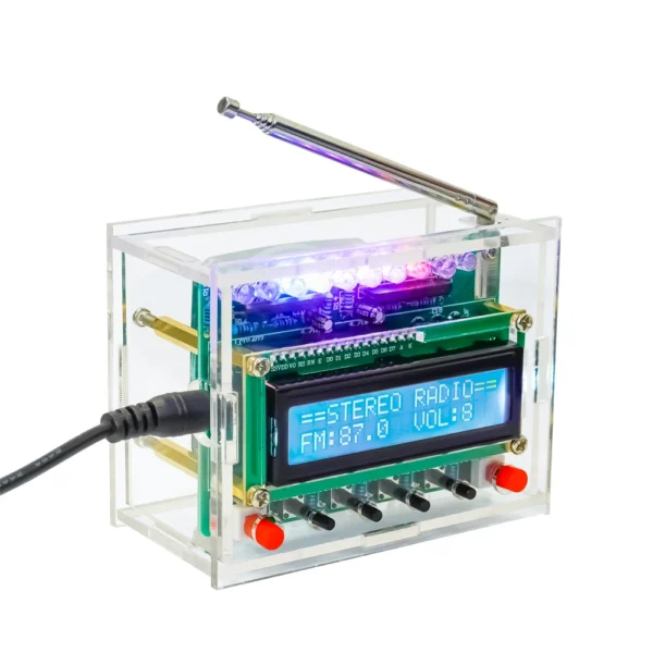 87-108MHz FM Digital Radio DIY Kit DIY Radio Soldering Components DA5807 LCD Display
$10.90
87-108MHz FM Digital Radio DIY Kit DIY Radio Soldering Components DA5807 LCD Display
$10.90
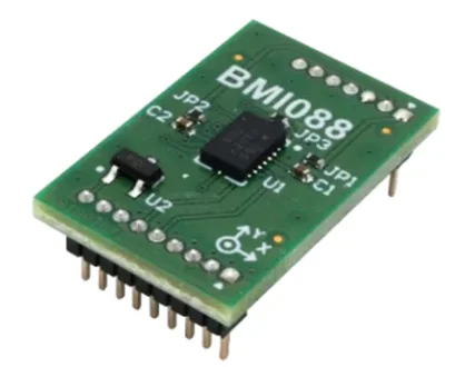 BMI088 Shuttle Board 3.0 BMI088 multifunctional sensor development tools
$33.90
BMI088 Shuttle Board 3.0 BMI088 multifunctional sensor development tools
$33.90
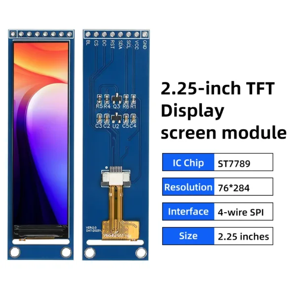 2.25-inch TFT LCD Small Screen Module ST7789 Screen 76*284 Module Full Viewing Angle SPI Color Screen 8-pin Blue Board Module
$6.90 – $7.90Price range: $6.90 through $7.90
2.25-inch TFT LCD Small Screen Module ST7789 Screen 76*284 Module Full Viewing Angle SPI Color Screen 8-pin Blue Board Module
$6.90 – $7.90Price range: $6.90 through $7.90
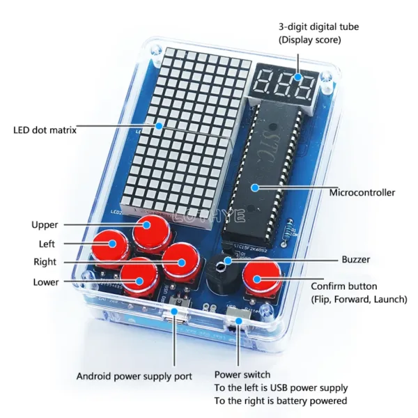 DIY Game Kit Retro Classic Electronic Production Kit Soldering Welding Tranning Set Snake Plane Racing Mini Pixel Game Console