If you have ever sat in a hardware procurement meeting or read financial reports on electronics manufacturing, you have likely heard the terms "PCB" and "PCBA" used interchangeably. This is a critical mistake.
While they differ by only two letters, confusing a Printed Circuit Board (PCB) with a Printed Circuit Board Assembly (PCBA) can lead to catastrophic supply chain miscommunications, incorrect budget forecasting, and severe manufacturing delays. For hardware engineers and purchasing managers, understanding the distinction is not just about vocabulary; it is about knowing exactly what you are buying, who is responsible for quality control, and how to optimize your path to mass production.
This guide cuts through basic textbook definitions. We will break down the technical and commercial differences between PCB and PCBA, analyze the manufacturing processes that bridge the gap between the two, and provide a strategic framework for choosing the right production model for your hardware.
The Core Distinction: Bare Board vs. Finished Product
To put it simply: PCBA = PCB + Components + Assembly Process.
What is a PCB? (The Foundation)
A Printed Circuit Board (PCB), often referred to as a "bare board" or "blank board," is the foundational substrate that mechanically supports and electrically connects electronic components. It is manufactured by etching conductive copper pathways (traces) onto a non-conductive substrate, most commonly FR-4 (glass-reinforced epoxy laminate).
At this stage, the PCB is entirely passive. It contains no intelligence, no power regulation, and no signal processing capability. It is merely a highly engineered component, much like a chassis or a housing, waiting to be populated.
What is a PCBA? (The Functional Unit)
A Printed Circuit Board Assembly (PCBA) is the result of taking a bare PCB and populating it with electronic components—such as integrated circuits (ICs), resistors, capacitors, and connectors—via a precise manufacturing process.
Once the components are soldered and the board has passed functional testing, it transitions from a mere component into a functional sub-assembly or a finished good. When you buy a computer motherboard or a smartphone logic board, you are buying a PCBA, not a PCB.
The Manufacturing Bridge: How a PCB Becomes a PCBA
The transformation from a bare board to a functional assembly is where the real engineering value—and the highest risk of defects—lies. Modern PCBA manufacturing relies on two primary methodologies, often used in tandem.
1. Surface Mount Technology (SMT)
SMT is the dominant assembly method for modern electronics, accounting for the vast majority of component placement. The process is highly automated and relies on strict process control:
- Solder Paste Printing: A laser-cut stainless steel stencil is aligned over the bare PCB. Solder paste (typically SAC305 for lead-free applications) is squeegeed through the stencil apertures onto the copper pads.
- SPI (Solder Paste Inspection): A 3D optical system immediately verifies the volume, height, and alignment of the deposited paste, catching up to 70% of potential defects before components are even placed.
- Pick and Place: High-speed robotic machines use vacuum nozzles to pick components from feeders and place them onto the tacky solder paste with micron-level accuracy.
- Reflow Soldering: The board travels through a multi-zone thermal oven. The carefully profiled temperature curve melts the solder paste, forming a permanent metallurgical and mechanical bond between the component leads and the PCB pads.
2. Through-Hole Technology (THT) & Wave Soldering
While SMT handles miniaturized components, certain parts—like heavy connectors, large capacitors, or components requiring high mechanical stress resistance—still require leads to be inserted through drilled holes in the PCB.
- Wave Soldering: The populated board passes over a standing wave of molten solder, which wicks up the component leads to form the joint.
- Selective Soldering: For mixed-technology boards (SMT on one side, THT on the other), programmable micro-nozzles apply solder only to specific through-hole pins, protecting nearby heat-sensitive SMT components from thermal shock.
The Procurement Reality: Make vs. Buy Decisions
Understanding the difference between PCB and PCBA directly impacts your supply chain strategy. Hardware teams generally face three procurement models, each with distinct trade-offs.
Model A: PCB-Only Procurement (In-House Assembly)
You purchase bare PCBs from a fabricator and source components separately, assembling them in-house or via a local shop.
- Pros: Maximum control over component sourcing; lower upfront NRE (Non-Recurring Engineering) costs for simple boards.
- Cons: You assume 100% of the quality risk. If a board fails, the PCB manufacturer will blame your assembly process, and your component supplier will blame the PCB pad finish. This "blame game" destroys project timelines.
Model B: Consignment Assembly
You purchase the bare PCBs and source all components yourself, then ship them to a Contract Manufacturer (CM) solely for the labor of assembly.
- Pros: You retain control over the BOM (Bill of Materials) and component costs.
- Cons: You are still responsible for component shortages, counterfeit risks, and logistics. The CM will charge a premium for managing your disparate material deliveries.
Model C: Turnkey PCBA Manufacturing (The Industry Standard)
You provide the Gerber files and BOM to a single manufacturer who handles everything: bare PCB fabrication, component procurement, SMT/THT assembly, and final testing.
- Pros: Single-point accountability. If the final PCBA fails, there is only one vendor responsible for fixing it. Turnkey providers leverage their massive purchasing power to secure better component pricing and guarantee authenticity.
- The Strategic Move: By utilizing a dedicated turnkey PCB prototype and assembly manufacturing service, you ensure that the Design for Manufacturability (DFM) feedback provided during your initial prototype run is directly baked into the mass-production process. This eliminates the costly "re-engineering" phase when scaling up.
The Hidden Cost of Poor PCB-to-PCBA Transition
A bare PCB might pass all electrical flying probe tests at the fabrication house, but still fail catastrophically during PCBA assembly. Why? Because the design was optimized for a bare board, not for assembly.
Common DFM failures that occur at the PCBA stage include:
- Insufficient Solder Mask Dams: Leading to solder bridging on fine-pitch ICs during reflow.
- Thermal Imbalance: Large ground planes connected directly to pads without thermal reliefs, acting as heat sinks and causing cold solder joints or component tombstoning.
- Poor Fiducial Placement: Preventing the SMT pick-and-place machine's vision system from accurately aligning components, leading to placement offset (or misalignment).
To prevent these issues, your PCB design must be reviewed against PCBA assembly capabilities before fabrication begins.
The Startup Advantage: Rapid Iteration Without Financial Risk
We understand that for hardware startups, independent developers, and research teams, the cost of multiple prototype iterations to validate the transition from PCB design to PCBA functionality can rapidly drain an R&D budget.
This is not a marketing gimmick; it is a strategic engineering tool. It allows you to:
- Validate Mechanical Fit: Test connector alignments, mounting holes, and enclosure clearances with real, production-grade FR-4 boards.
- Iterate Fearlessly: Test different component footprints, thermal via patterns, or SMT pad designs without financial penalty.
- Accelerate R&D: Order multiple layout variants simultaneously to compare real-world assembly and testing results.
Scaling Up: From Prototype to OEM/ODM Mass Production
Once your PCBA design is validated and your DFM issues are resolved, the focus shifts to supply chain resilience, cost optimization, and consistent quality at volume.
Transitioning from a 10-piece prototype to a 10,000-unit production run requires a partner who can secure long-lead component allocation, optimize panelization (using V-scores or mouse bites) to reduce material waste, and implement rigorous Statistical Process Control (SPC) on the SMT line.
If you are preparing to scale your product line, initiating an OEM/ODM bulk manufacturing inquiry early in your design cycle allows our engineering team to align your BOM and layout with the most cost-effective and scalable production methodologies from day one. Consolidating your supply chain under one roof drastically reduces lead times and eliminates the logistical friction of managing multiple vendors.
Frequently Asked Questions (FAQ)
Q: Can a PCB manufacturer also handle the full PCBA process?
A: Yes. Reputable electronics manufacturers offer "turnkey" services, meaning they handle the bare PCB fabrication, source all components from authorized distributors, and perform the complete SMT/THT assembly and testing under one roof.
Q: Why is my bare PCB passing tests, but failing after PCBA assembly?
A: This is almost always a Design for Manufacturability (DFM) issue. Common culprits include poor thermal relief design causing cold joints, insufficient annular rings leading to via breakout during drilling, or pad sizes that do not match the component's recommended land pattern, causing tombstoning during reflow.
Q: What is the difference between SMT and Through-Hole (THT) assembly?
A: SMT (Surface Mount Technology) places components directly onto the surface of the PCB pads, allowing for higher density and full automation. THT (Through-Hole Technology) involves inserting component leads through drilled holes in the PCB, offering superior mechanical strength for heavy connectors or high-stress applications, but requiring more manual labor or specialized wave soldering.
Q: How do I ensure my PCBA manufacturer uses authentic components?
A: Always partner with a turnkey manufacturer that sources exclusively from tier-1, franchised distributors (like Digi-Key, Mouser, or Arrow). They should be able to provide full lot traceability and Certificates of Conformity (CoC) for critical components upon request.
Stop Guessing, Start Manufacturing with Confidence
Understanding the difference between a PCB and a PCBA is the first step in taking control of your hardware supply chain. A brilliant circuit design is only as good as the manufacturing process that brings it to life. By partnering with a manufacturer that enforces strict DFM rules, maintains transparent supply chains, and offers seamless turnkey solutions, you eliminate costly respins and accelerate your time-to-market.
Whether you are utilizing our $2 for 5 pieces (under 50x50mm) offer to validate your initial layout, or you are ready to scale a complex, mixed-technology design into high-volume production, our engineering team is prepared to provide the actionable feedback and precision manufacturing your project demands.
Ready to build with confidence?
Reach out to our engineering team today for a comprehensive DFM review and a precise manufacturing quote. Let's engineer a product that performs flawlessly in the field.

 Deauther Watch X II - ESP8266 Development Watch
$36.90
Deauther Watch X II - ESP8266 Development Watch
$36.90
 YH-TC05 DC12-24V Tachometer Counter Electronic Digital Display Tachometer Gauge Sensor Non-Contact Motor Speed Meter with Modbus
$2.60 – $15.90Price range: $2.60 through $15.90
YH-TC05 DC12-24V Tachometer Counter Electronic Digital Display Tachometer Gauge Sensor Non-Contact Motor Speed Meter with Modbus
$2.60 – $15.90Price range: $2.60 through $15.90
 SenseCAP S700-B 7-in-1 Compact Weather Station with Solar Radiation Shield,Temp,Humidity,Rain,Wind,Pressure,Ultrasonic& Optical
$1,000.00
SenseCAP S700-B 7-in-1 Compact Weather Station with Solar Radiation Shield,Temp,Humidity,Rain,Wind,Pressure,Ultrasonic& Optical
$1,000.00
 1.3inch LCD Display Module, Embedded ST7789 Driver, Using SPI Bus. For Raspberry Pi Pico
$9.90
1.3inch LCD Display Module, Embedded ST7789 Driver, Using SPI Bus. For Raspberry Pi Pico
$9.90
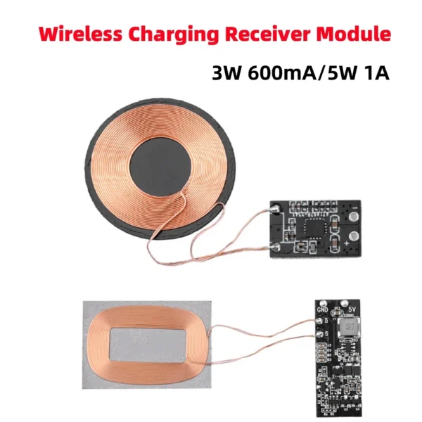 3W 600mA/5W 1A Wireless Charging Receiver Module Small Coil Built-in 5V Charging Wireless Charger PCBA Board
$2.60 – $2.90Price range: $2.60 through $2.90
3W 600mA/5W 1A Wireless Charging Receiver Module Small Coil Built-in 5V Charging Wireless Charger PCBA Board
$2.60 – $2.90Price range: $2.60 through $2.90