There is a well-known adage in hardware engineering: "PCB design is 90% component placement and 10% routing." While modern EDA tools have made trace routing highly automated, component placement remains a deeply manual, strategic process.
For hardware engineers and product managers, a poorly planned layout is not just an aesthetic issue—it is a direct threat to your bottom line. A chaotic placement strategy leads to SMT nozzle collisions, wave soldering shadowing effects, automated optical inspection (AOI) blind spots, and catastrophic signal integrity failures. Ultimately, these layout flaws force expensive board respins and inflate mass-production assembly costs.
This guide moves beyond basic textbook theories. We will break down the 10 critical Design for Manufacturability (DFM) rules for PCB component placement, ensuring your design transitions smoothly from a digital schematic to a high-yield, cost-effective physical product.
The 10 Commandments of Professional PCB Component Placement
1. Lock Down Mechanical Constraints and Keep-Out Zones First
Before placing a single IC, you must define the physical boundaries of your board. Lock the positions of mounting holes, edge connectors, USB ports, and mechanical switches. Crucially, establish strict Keep-Out Zones for V-score lines, tab-routing (mouse bites), and panelization rails. Failing to respect these mechanical constraints will result in boards that cannot be mounted in their enclosures or depanelized without stressing edge-mounted ceramic capacitors.
2. Design for the Assembly Process (SMT vs. Wave Soldering)
Your placement strategy must align with your chosen soldering process. If your board utilizes Through-Hole Technology (THT) and will undergo wave soldering, component orientation is critical.
- The Shadowing Effect: If a tall component is placed directly behind a smaller component (relative to the direction of the solder wave), the tall component will "shadow" the smaller one, blocking the solder flow and causing cold joints. Always align components parallel to the wave direction and maintain adequate spacing to prevent this.
3. Respect the Component Courtyard and SMT Nozzle Clearance
Modern high-density designs often push components dangerously close together. According to IPC-7351 standards, every component footprint must include a "courtyard"—a designated keep-out area around the part. Maintaining a minimum clearance (typically ≥0.25mm to 0.5mm) between courtyards ensures that the SMT pick-and-place machine’s vacuum nozzles have enough physical space to pick and place parts without colliding with adjacent, already-placed components.
4. Standardize Component Orientation and Polarity
While it may seem trivial, standardizing the orientation of identical components (e.g., all 0402 resistors facing the same direction, all ICs with Pin 1 in the top-left corner) drastically reduces assembly errors.
- For SMT: It simplifies the pick-and-place programming and reduces the number of feeder rotations, shaving seconds off the cycle time per board.
- For AOI and Manual Inspection: Uniform polarity makes it exponentially easier for AOI algorithms and human inspectors to instantly spot reversed diodes, tantalum capacitors, or misaligned ICs.
5. Minimize Ratsnest Crossings for Signal Integrity
In your EDA software, unrouted connections are displayed as "ratsnest" lines. While minimizing these crossings speeds up the routing phase, it is fundamentally about Signal Integrity (SI) and Power Integrity (PI). By logically grouping components based on the schematic (e.g., keeping the MCU, its decoupling capacitors, and the crystal oscillator tightly clustered), you minimize trace lengths, reduce parasitic inductance, and prevent high-speed signals from crossing split ground planes.
6. Prioritize Single-Sided SMT Assembly
Every time a PCB needs to be flipped to solder components on the bottom layer, the assembly cost and cycle time increase. It requires a second solder paste printing, a second pass through the pick-and-place machine, and a second reflow cycle (often requiring adhesive or specialized solder paste to hold bottom-side parts). Whenever possible, consolidate all SMT components on the top layer to enable a single-pass, highly cost-effective assembly process.
7. Optimize for Automated Optical Inspection (AOI) and Testing
A brilliant circuit is useless if it cannot be tested.
- AOI Visibility: Ensure that tall components do not cast physical shadows over smaller adjacent components, blocking the AOI cameras' line of sight.
- Test Point Placement: Distribute test points evenly across the board and maintain a minimum clearance (typically ≥0.5mm) from tall components to allow the ICT (In-Circuit Test) bed-of-nails fixture to make reliable contact without the probe tips slipping.
8. Prevent Solder Bridging via Smart Footprint Spacing
Never compromise on pad spacing to save board real estate. Placing components too closely, or routing traces too close to component pads without adequate solder mask dams, invites solder bridging during reflow. For fine-pitch ICs (like QFNs or BGAs), ensure the footprint strictly adheres to the manufacturer’s recommended land patterns to prevent solder wicking and short circuits.
9. Group by Functional Blocks and Thermal Management
Treat your PCB layout like a city grid. Group analog components away from noisy digital switching circuits (like DC-DC converters) to prevent EMI coupling. Furthermore, identify high-power dissipation components early in the placement phase. Position them near board edges, thermal vias, or dedicated copper pours to facilitate heat dissipation, ensuring they do not thermally degrade nearby temperature-sensitive components.
10. Validate with 3D MCAD Integration and DFM Software
Do not rely solely on 2D views. Modern EDA tools allow for 3D Mechanical CAD (MCAD) integration. Use this to verify that tall components do not collide with the enclosure lid, and that connectors align perfectly with the mechanical housing. Finally, run your layout through a dedicated DFM analysis tool to automatically flag manufacturing violations before you ever send the Gerber files to the factory.
The Hidden Cost of Poor Layout: Why Prototyping Strategy Matters
A layout that looks perfect on a 2D screen can fail spectacularly in the real world due to mechanical interference, thermal hotspots, or unexpected EMI issues. Iterating through multiple layout revisions to fix these physical flaws can rapidly drain an R&D budget.
This is not a gimmick; it is a strategic engineering tool. It allows you to:
- Validate Mechanical Fit: Print the board to test connector alignments and mounting hole clearances in your actual enclosure.
- Iterate Fearlessly: Test different component groupings or thermal via placements without financial penalty.
- Accelerate R&D: Order multiple layout variants simultaneously to compare real-world thermal and EMI performance.
Scaling Your Design: From Layout to Turnkey Manufacturing
Once your component placement is optimized and validated, the focus shifts to supply chain execution. A flawless layout can still be ruined by poor stencil design, misaligned pick-and-place files, or counterfeit components.
Transitioning from a validated prototype to mass production requires a partner who understands the intricacies of your layout. By utilizing our turnkey PCB prototype and assembly manufacturing services, you ensure that the DFM feedback provided during the prototyping phase is directly translated into optimized stencils and precise SMT programming for your production run.
If you are preparing to scale your product line, initiating an OEM/ODM bulk manufacturing inquiry early allows our engineering team to review your layout for panelization efficiency, ensuring you get the maximum number of boards per panel, drastically reducing your per-unit assembly cost.
FAQ
Q: What is the "shadowing effect" in PCB component placement?
A: The shadowing effect occurs during wave soldering when a tall component is placed directly behind a shorter component relative to the direction of the solder wave. The tall component blocks the solder flow, resulting in cold or insufficient solder joints on the smaller component.
Q: Why is component orientation important for SMT assembly?
A: Standardizing component orientation reduces pick-and-place machine rotation time, speeds up the assembly cycle, and makes it significantly easier for Automated Optical Inspection (AOI) systems to quickly identify reversed or missing parts.
Q: How does component placement affect PCBA testing?
A: Poor placement can block AOI cameras from viewing small components or prevent ICT (In-Circuit Test) probes from making physical contact with test points. Maintaining adequate clearance around test points ensures 100% test coverage.
Q: Can your facility review my PCB layout for DFM before manufacturing?
A: Yes. As a comprehensive turnkey manufacturer, our CAM engineers perform a thorough DFM review on all incoming Gerber files. We will flag component spacing violations, insufficient solder mask dams, and test point accessibility issues before production begins.
Stop Letting Poor Layout Dictate Your Manufacturing Costs
Mastering PCB component placement is the single most effective way to reduce assembly costs, eliminate field failures, and accelerate your time-to-market. It requires a deep understanding of both electrical design and physical manufacturing constraints.
Whether you are utilizing our $2 for 5 pieces (under 50x50mm) offer to validate your mechanical layout, or you are ready to scale a complex, high-density design into mass production, our engineering team is prepared to provide the actionable DFM feedback and precision manufacturing your project demands.
Ready to build with confidence?
Reach out to our engineering team today for a comprehensive DFM review of your layout and a precise manufacturing quote. Let's engineer a board that is as easy to manufacture as it is brilliant in design.

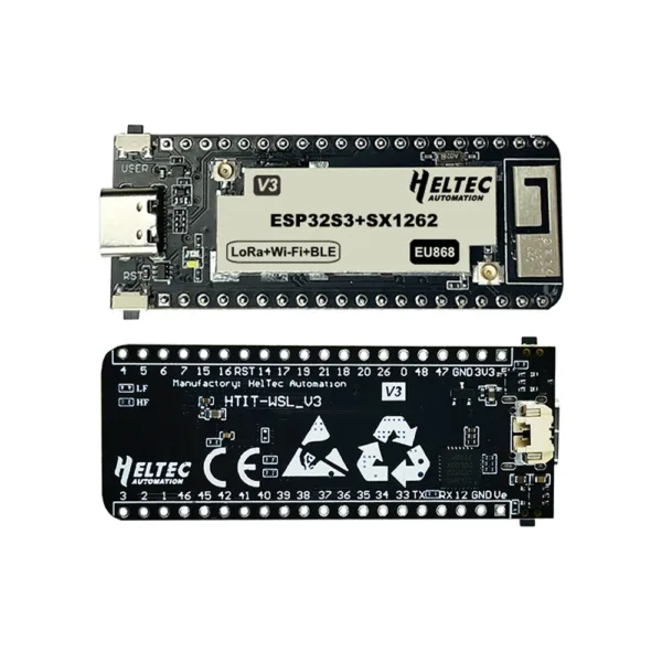 433-510MHZ/ 863-928MHZ Wireless stick lite ESP32+LoRa V3 development board compatible with ESP32-S3 node Type - C
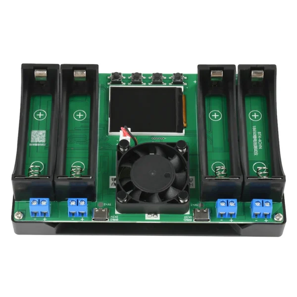 18650 Lithium Battery Capacity Tester
$10.90
18650 Lithium Battery Capacity Tester
$10.90
 ESP32-S3 ETH Camera Development Board PoE RJ45 / OV2640 OV5640 Port / W5500 / Micro-SD Compatible With Raspberry Pi Pico Size
 Ideal Diode Module Adopts 12V 24V 36V 48V Voltage Irrigation Battery Charging Anti Backflow Protection
$4.50
Ideal Diode Module Adopts 12V 24V 36V 48V Voltage Irrigation Battery Charging Anti Backflow Protection
$4.50
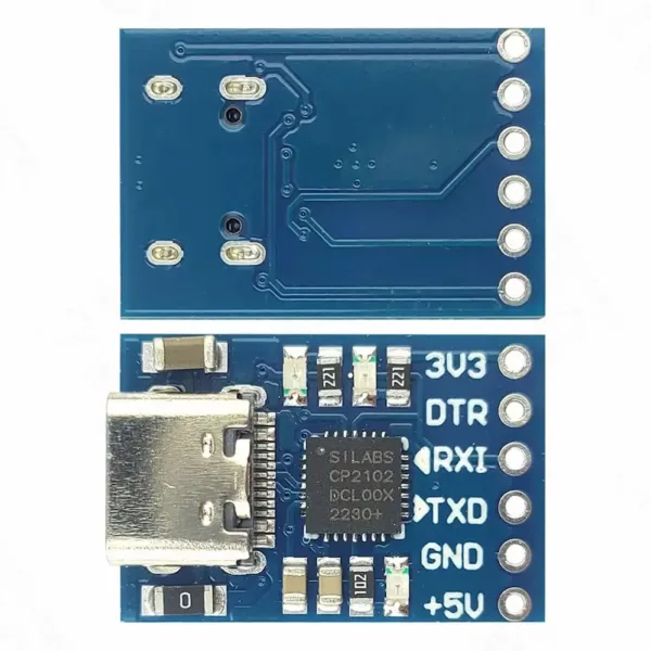 MINI USB TO TTL Serial Downloader Converter UART STC Download USB Micro Type-C 6Pin UART STC 300bps~1Mbps CP2102