Integrated Circuit (IC) packages are not merely mechanical housings; they are the primary physical constraints that dictate a product's PCB stack-up, thermal management strategy, SMT process window, and inspection methodology.集成电路(IC)封装不仅仅是机械外壳;它们还是决定产品PCB叠层设计、热管理策略、SMT工艺窗口以及检测方法的主要物理约束。
When PCBA designs transition from schematic to mass production, recurring yield losses frequently trace back to a fundamental disconnect: the hardware design treated the IC package purely as a CAD footprint, ignoring the physical realities of solder paste rheology, reflow thermodynamics, and X-ray inspection limits.当PCBA设计从原理图阶段进入批量生产时,反复出现的良率损失往往源于一个根本性的脱节:硬件设计仅将IC封装视为CAD中的封装焊盘布局,而忽视了焊膏流变特性、回流焊接热力学以及X射线检测局限等实际物理因素。
This document details the manufacturing constraints and Design for Manufacturability (DFM) requirements for the twelve most common IC package families, providing the specific process controls needed to ensure reliable assembly.本文详细阐述了十二种最常见集成电路封装系列的制造限制与可制造性设计(DFM)要求,并提供了确保可靠组装所需的具体工艺控制措施。
1. Through-Hole and Gull-Wing Packages (DIP, SOP, QFP/LQFP)1. 贯穿孔与鸥翼型封装(DIP、SOP、QFP/LQFP)
These packages feature external leads (gull-wing or straight pins) that are visible and probe-able, making them generally forgiving for assembly and inspection. However, as pin pitch decreases, the process window narrows significantly.
DIP (Dual In-Line Package)
- Process Reality: Requires wave soldering or manual soldering. Incompatible with modern double-sided SMT assembly.
- DFM Constraint: Occupies significant board real estate. For production volumes exceeding 1,000 units, DIP should be avoided unless specifically required for field serviceability or high-mechanical-stress applications.
SOP (Small Outline Package) & QFP/LQFP (Quad Flat Package)
- Process Reality: Compatible with standard SMT processes. Standard SOP uses a 1.27mm pitch, while fine-pitch QFP/LQFP reduces this to 0.5mm or 0.4mm.
- DFM Constraint: At pitches ≤0.5mm, the lead width is approximately 0.2mm. Solder bridging becomes a primary defect mode if stencil aperture reduction is not precisely calculated.
- Inspection & Control: Fine-pitch QFP requires 100% Automated Optical Inspection (AOI). However, AOI cannot always detect the actual solder fillet under the meniscus; therefore, strict Solder Paste Inspection (SPI) before component placement is mandatory to control paste volume. Additionally, component lead coplanarity must be strictly controlled (typically <0.1mm) to prevent floating (open) joints on the longest leads.
2. Leadless Packages (QFN/DFN): Thermal Management and Voiding
QFN (Quad Flat No-lead) and DFN packages eliminate external leads, placing solderable terminations on the perimeter and a large exposed thermal pad on the bottom. This architecture offers superior electrical performance (low parasitic inductance) but introduces severe inspection and process challenges.
- The Voiding Defect: During reflow, flux volatiles trapped under the large thermal pad expand. If the PCB layout features a solid copper pad with no escape routes, the gas creates massive voids. A voiding rate exceeding 25% (and often 15% for power devices) drastically increases thermal resistance, leading to field failures.
- DFM Constraints:
- Stencil Design: The stencil aperture for the thermal pad must utilize a window-pane or cross-hatch pattern, covering only 50% to 70% of the pad area to allow gas escape.
- PCB Layout: The thermal pad must be stitched with an array of thermal vias (typically 0.3mm diameter, 1.0mm pitch) to provide a path for trapped gases to vent into inner layers.
- Inspection: AOI is blind to the thermal pad solder joint. 100% X-ray inspection is mandatory for automotive, medical, and high-reliability applications to verify voiding percentages.
3. Array and Miniature Packages (BGA, CSP/WLCSP)
When moving to Ball Grid Array (BGA) or Wafer-Level Chip Scale Package (WLCSP), all visual inspection capabilities are lost. The solder joints are entirely hidden beneath the component body.
BGA (Ball Grid Array)
- Process Reality: Enables pin counts from 100 to over 2,000. The large thermal mass of BGAs requires extended soak times in the reflow profile to ensure all balls reach liquidus simultaneously.
- DFM Constraint: A common defect is "Head-in-Pillow" (HIP), where the BGA ball and PCB pad melt but fail to coalesce due to flux exhaustion or pad oxidation. Preventing HIP requires strict Moisture Sensitivity Level (MSL) baking protocols and a reflow profile with a controlled ramp rate through the liquidus phase.
- Inspection: 100% X-ray inspection is required to detect bridging, insufficient wetting, and voiding. For BGAs larger than 15mm x 15mm, or in high-vibration environments, capillary underfill is mandatory to prevent solder joint fatigue.
CSP / WLCSP (Wafer-Level Chip Scale Package)
- Process Reality: The package dimension is within 20% of the bare die size.
- DFM Constraint: WLCSP devices have zero mechanical compliance. They are highly susceptible to solder joint cracking caused by PCB flexure during depaneling or Coefficient of Thermal Expansion (CTE) mismatch during thermal cycling.
- Control: Capillary underfill is strictly required. Furthermore, WLCSP components must never be placed near board edges, connectors, or mounting holes where mechanical stress is concentrated.
4. High-Performance Packages (LGA, FCBGA)
For high-end computing and server applications, Flip-Chip BGA (FCBGA) and Land Grid Array (LGA) are the standard. These packages are massive and unforgiving.
- Package Warpage: An FCBGA can exceed 50mm x 50mm. During reflow, the thermal gradient between the center and the edges causes the package to warp (smile or frown). If the warpage exceeds the coplanarity of the solder balls, the center joints will fail to contact the PCB pad.
- DFM Constraint: Mitigating warpage requires a highly optimized reflow profile with forced convection to minimize the delta-T across the package. Additionally, the CTE mismatch between the organic substrate and standard FR-4 can cause severe reliability issues; low-CTE materials (e.g., Megtron 6) and symmetrical stack-ups are often required.
Validating Process Windows Through Physical Prototyping
Simulation and datasheet analysis can predict electrical performance, but they cannot reveal assembly defects, thermal hotspots, or mechanical stress concentrations. Physical prototyping is essential to validate QFN thermal via venting, BGA reflow profiles, and WLCSP underfill capillary flow.
This allows engineering teams to build dedicated test coupons, run them through the SMT line, and verify X-ray voiding rates on the actual stack-up before committing to the main board layout.
Transitioning to Volume Production
Once the prototype validates the package selection and footprint design, scaling to mass production requires a partner who understands the inspection and process control requirements for each package type.
Our turnkey PCB prototype and assembly manufacturing service ensures that the exact stencil designs, reflow profiles, and inspection criteria validated during prototyping are locked into the production control plan. We maintain dedicated X-ray and AOI inspection lines calibrated for fine-pitch QFN, BGA, and WLCSP devices.
When transitioning to high-volume production, initiating an OEM/ODM bulk manufacturing inquiry allows our process engineering team to optimize panelization for your specific package mix, secure long-term component allocation, and implement statistical process control (SPC) on critical parameters like BGA voiding and QFN solder joint coverage.
FAQ
Q: What is the minimum annular ring required for QFN thermal vias?
A: For reliable via-in-pad construction under QFN thermal pads, maintain a minimum annular ring of 0.10mm (4 mil). The via diameter should be 0.30mm (12 mil) or smaller, with a pitch of 0.8-1.0mm to prevent solder wicking.
Q: What is the maximum acceptable voiding percentage for BGA and QFN thermal pads?
A: Per IPC-A-610 Class 2 (commercial) and Class 3 (automotive/medical), the maximum voiding for BGA balls and QFN thermal pads is 25% of the total joint area. For high-power or high-reliability applications, we target <15% voiding through optimized stencil design and reflow profiling.
Q: When is underfill required for BGA and WLCSP packages?
A: Underfill is mandatory for WLCSP devices, for BGAs larger than 15mm x 15mm, and for any BGA in high-vibration or thermal cycling environments. It prevents solder joint fatigue failure due to CTE mismatch between the silicon substrate and the FR-4 PCB.
Q: Can standard AOI inspect QFN solder joints adequately?
A: AOI can inspect the perimeter joints of QFN packages but cannot verify the thermal pad soldering. X-ray inspection is required to check for voiding, insufficient solder, and bridging under the thermal pad. For automotive applications, 100% X-ray is standard practice.
Package selection is a foundational decision that cascades through every stage of product development—from PCB layout and thermal design to assembly yield and field reliability. Understanding the manufacturing implications of each package type allows for informed trade-offs between performance, cost, and producibility.
If your next design involves high-density BGAs, fine-pitch QFNs, or thermal-critical power devices, our engineering team is ready to review your footprints and assembly drawings. We will identify DFM issues related to package selection, thermal via patterns, and inspection accessibility to ensure your design transitions smoothly from prototype to mass production.

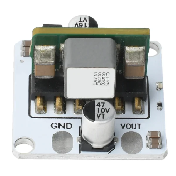 DC 9-16V to 5V Converter 10A 50W Module Buck Regulator Step Down Board Voltage Power Supply Accessory
$2.30
DC 9-16V to 5V Converter 10A 50W Module Buck Regulator Step Down Board Voltage Power Supply Accessory
$2.30
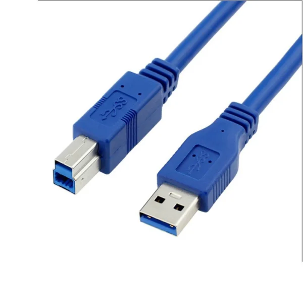 USB 3.0 A Male AM to USB 3.0 B Type Male BM USB3.0 Cable 0.3m 0.6m 1m 1.5m 1.8m 3m 5m 1ft 2ft 3ft 5ft 6ft 10ft 30cm 1 3 5 Meters
$1.90 – $5.60Price range: $1.90 through $5.60
USB 3.0 A Male AM to USB 3.0 B Type Male BM USB3.0 Cable 0.3m 0.6m 1m 1.5m 1.8m 3m 5m 1ft 2ft 3ft 5ft 6ft 10ft 30cm 1 3 5 Meters
$1.90 – $5.60Price range: $1.90 through $5.60
 Smart WiFi/ZigBee PIR Motion Sensor - Wireless Infrared Security Detector, APP Alerts, Smart Home Burglar Alarm System
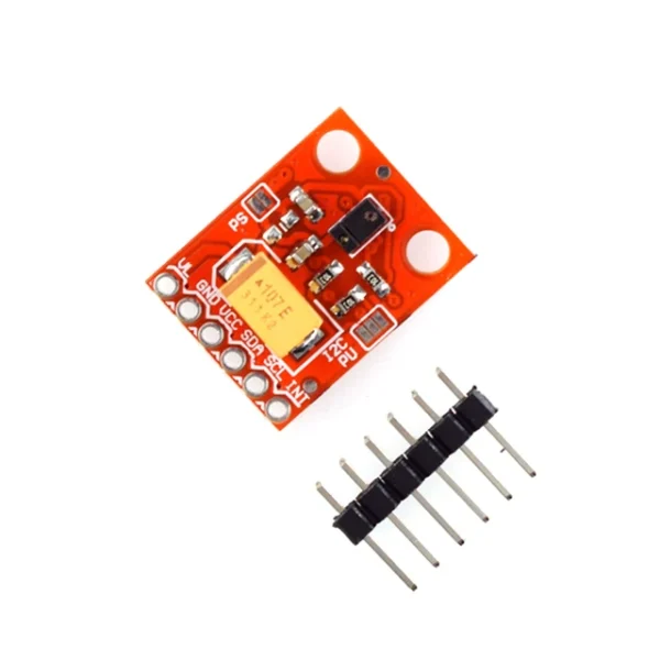 GY-9960 APDS-9960 3.3V Proximity Detection And Non-Contact Gesture Detection RGB Attitude Sensor For Arduino I2C IIC Breakout
$4.90
GY-9960 APDS-9960 3.3V Proximity Detection And Non-Contact Gesture Detection RGB Attitude Sensor For Arduino I2C IIC Breakout
$4.90
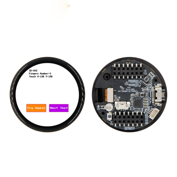 LILYGO T-Display-S3 ESP32-S3 1.43-inch AMOLED Development Board WiFi Bluetooth Wireless Module Flash 16MB PSRAM 8MB For Arduino
$28.90 – $38.90Price range: $28.90 through $38.90
LILYGO T-Display-S3 ESP32-S3 1.43-inch AMOLED Development Board WiFi Bluetooth Wireless Module Flash 16MB PSRAM 8MB For Arduino
$28.90 – $38.90Price range: $28.90 through $38.90