
nRF52840 PCB Layout for BLE Products: Antenna, Matching, and Certification
The nRF52840 is one of the most popular BLE and multiprotocol chips in the world, and for good reason: it
Your firmware works. The serial log prints clean, the sensor reads true, and the board boots every time. Then you walk ten feet away from the router and the connection dies.
If that sounds familiar, you are not alone. Every week, engineers move a working ESP32 dev board design onto a custom PCB, and the radio that reached across the house suddenly reaches across the room. The chip is identical. The sketch is identical. The only thing that changed is the board underneath it.
More often than not, the culprit is not the chip, the power supply, or the firmware. It is the space immediately around the antenna — the one region on your board that has to stay empty, and the one region almost everyone fills with copper.
This guide walks through the seven layout mistakes that quietly gut 2.4 GHz performance, what each one actually does to the antenna, and how to correct it. It is written for people doing real hardware: module-based designs on two- and four-layer boards, headed to a prototype or a first production run.
An ESP32 module antenna is not a simple piece of metal. It is a tuned radiating element, and its resonant frequency depends on the electromagnetic environment directly around it. That environment is your PCB.
The inverted-F antenna on a module like the ESP32-WROOM-32E is cut to resonate at roughly 2.4 GHz. Put a ground pour underneath it, or a battery beside it, and you change the effective electrical length of the antenna. It detunes. Your transmitter is still pushing watts into the air — but the antenna is no longer listening at the right frequency, so the energy goes nowhere useful.
Everything below comes back to that one idea: the antenna needs empty space, and conductive material steals it. Espressif publishes exact keep-out dimensions for every module in its hardware design guidelines. Design to those figures instead of estimating, because a couple of millimetres of intruding copper is enough to show up in a range test.
This is the single most common cause of weak Wi-Fi on custom ESP32 boards, and it is the easiest to fix once you know to look for it.
The rule is absolute: no copper of any kind on any layer beneath or beside the antenna. That means ground pours, power planes, signal traces, copper fills, and even the ground stitching vias you added everywhere else because they are good practice. In the keep-out region, they are not.
The reason people get this wrong is that a solid ground plane under the whole board is a habit — and a good habit, almost everywhere else. On a digital board, more ground is almost always better. Under an antenna, it is a short circuit to performance. The copper couples to the radiating element, shifts its resonance, and absorbs energy that should be leaving the board.
The fix: carve the keep-out region out of every copper layer, not just the top. If your EDA tool supports copper keep-outs or design rules, set one up so it survives edits and reroutes. Then check it again after your final cleanup pass, because pours have a way of creeping back in.
Placement matters as much as the keep-out. An antenna radiates outward, and it does not care that your board has a neat, symmetrical layout. If the module sits in the centre of a large PCB, the antenna radiates partly into the board itself and partly into whatever is on the other side.
The recommended placement is unambiguous: put the module at the board edge, with the antenna end facing outward — ideally overhanging the edge of the carrier board entirely. The feed point should sit as close to that edge as your mechanics allow.
If the antenna genuinely cannot extend past the board edge, the next best option is to place the feed point near the edge and cut away the board on both sides of and beneath the antenna, opening up a clearance area. Do not hollow out the board on all four sides to create clearance around a centre-mounted module. That arrangement is specifically called out as not recommended in Espressif's guidelines, and for good reason: it fails to give the antenna a clean direction to radiate into.
The fix: decide module placement early, in the mechanical concept, not at the routing stage. By the time you are placing decoupling caps, it is often too late to move the module without reworking the enclosure.
You can follow every keep-out rule on the PCB and still lose range — because the PCB is not the whole RF environment. The enclosure is.
A plastic case is close to transparent at 2.4 GHz and is usually the right choice. A metal case blocks the signal almost entirely and forces you onto an external antenna. But even inside a plastic enclosure, the antenna needs breathing room from metal screws, stands, brackets, shields, display bezels, and internal metalwork.
Espressif recommends keeping at least 15 mm of clearance around the PCB antenna in all directions inside the final product. That is a mechanical constraint, and it needs to be agreed with whoever owns the enclosure — early, before tooling.
The fix: treat the keep-out area as a three-dimensional volume, not a 2D region on the layout. Sketch it onto the mechanical drawing. If the product will be housed in metal, or the antenna cannot see open space, plan for a U.FL variant module (ESP32-WROOM-32UE) and an external antenna from the start.
The moment you route RF from the module to a U.FL connector, or design your own antenna on a bare chip, the RF trace becomes a communication line with a specific impedance requirement: 50 Ω, with a tolerance of plus or minus 10 percent.
Engineers rarely get this wrong on purpose. It happens because a "50 Ω trace" is not a width — it is a width for a given stackup. Change the dielectric thickness, the copper weight, or the material, and the same trace width is no longer 50 Ω. Copy a width from an online calculator without matching your own stackup, and you have designed a mismatched line without noticing.
Mismatch means reflections. Reflections reduce transmitted power and degrade receive sensitivity, and they show up as an EVM that will not come in, or a link that works on the bench and fails in the field.
The fix: use a controlled-impedance stackup, get the trace geometry from your fabricator's impedance calculator for that exact stackup, and keep the RF trace short, straight, and free of stubs. No right-angle kinks — use gentle bends or mitred corners. Surround the trace with ground copper and stitching vias, and make sure there is a continuous ground reference directly beneath it with no plane splits under the RF path.
The crystal is the heartbeat of the whole radio. Its accuracy and cleanliness set the reference for both transmit and receive, and it is far more sensitive to layout than its small package suggests.
The classic failure mode: the design runs fine for a while, then TX performance degrades in ways that make no sense. The cause is often a crystal corrupted by a neighbouring signal — a high-speed line routed underneath it, a switching regulator placed too close, or an inductor or antenna radiating into it. RF performance drops, and the engineer spends a week debugging firmware that was never the problem.
The fix: keep the crystal close to the chip, with short, direct traces and its load capacitors placed as close to the crystal pins as physically possible. Route no high-speed or noisy signals beneath it, on any layer. Keep inductors, antennas, and other radiating parts well away. If you are designing with a bare chip rather than a module, this task becomes yours entirely — the module already handles it internally.
Weak Wi-Fi is not always an antenna problem. The radio is one of the hungriest, spikiest loads on the board, and a supply that looks clean on a multimeter may still be starving it at the moment of transmission.
The ESP32 draws sharp current bursts during TX. If the supply rail sags under that load, or if it carries noise from a nearby switcher, TX performance falls even though the rest of the board is happy. The symptom — poor range, dropped packets, occasional resets under load — gets misdiagnosed as an antenna issue month after month.
The fix: follow the decoupling shown in the reference schematic for your module, and place those capacitors close to the supply pins. Keep switching regulators and their loops away from the module and the antenna. On battery-powered designs, pay particular attention to the bulk capacitance that has to supply those TX bursts, and verify the rail with a scope under real transmit conditions rather than at idle. If you want a deeper walk-through of supply architecture for wireless boards, our ESP32 PCB Design service covers power planning as part of the circuit work.
Here is a mistake that is not really a mistake in the layout at all: assuming the layout is correct because it looks correct.
A design can follow every guideline above and still fall short, because real boards have real variables — the exact stackup your fabricator delivers, the enclosure that arrives from the moulding shop, the battery that gets added in revision two. A layout that passed the checklist can still underperform once the physical unit exists.
The step that catches this is final RF verification: throughput and communication-range testing on the assembled product, not just on the bare board. Espressif recommends exactly this. It is also the step teams skip when schedule pressure builds, and it is the one that would have caught the problem before the launch.
The fix: build the test into the plan. Bring up the first prototype with a range and throughput check before you commit to production volumes. On module-based designs, you inherit Espressif's modular certification — but "certified module" and "verified end product" are two different things, and only one of them is about your board.
If you are about to release a custom ESP32 board for fabrication, run through this:
Antenna layout is one of those disciplines where the rules fit on one page and the mistakes take weeks to find. Most of the cost of a bad RF layout is not the boards — it is the respin, the slipped schedule, and the launch that goes out with a range spec you cannot meet.
If you already have a schematic and need the board designed around it — placement, routing, and fabrication outputs ready to hand to your manufacturer — that is exactly what our PCB layout service is for. We lay out ESP32 carrier boards, sensor nodes, and connected products with the antenna, power, and crystal treated as RF, not as afterthoughts, and we hand over the source files, Gerbers, and a clear record of anything that needs your confirmation.
If your circuit is not defined yet — you know what the product must do, but not which module, power architecture, or connector set gets you there — start with our ESP32 PCB Design service instead. We work from a product brief through module selection, circuit design, layout, and prototype handoff.
Once the design is ready, the manufacturing step is a separate problem, and it should not be a slow one. We route fabrication and assembly through our online PCB and PCBA ordering, where you can upload Gerbers, pick your material, layer count, surface finish, and impedance control, and get boards moving — with FR-4 for standard work and Rogers or PTFE available when the design calls for a low-loss substrate.
Wi-Fi range on a custom ESP32 board is decided long before the firmware runs. Give the antenna empty space, put the module at the edge, respect the 50 Ω feedline and the crystal, feed the radio a clean rail, and verify the finished product — not the bare board. Do those things and the dev board performance you designed around will show up on the real thing.
Need a layout review before you commit to fabrication? Send us your project brief at [email protected] — or contact us online — and we will tell you what we see.
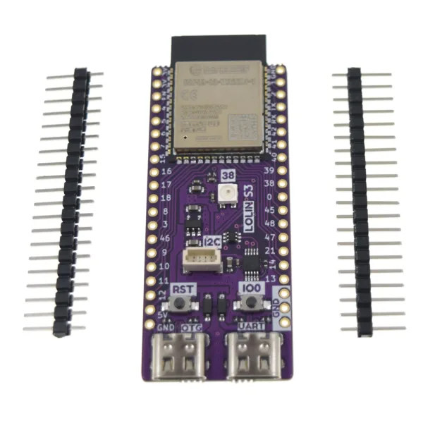 S3 V1.0.0 - LOLIN WIFI BLE IOT Board based ESP32-S3-WROOM-1 ESP32-S3 16MB FLASH 8MB PSRAM MicroPython Arduino Compatible
 eXtremeRate Whole Clicky Kit V2 for ps5 Controller BDM-040/050 Shoulder Face Dpad Buttons, Micro Switch Clicky Hair Trigger Kit
 PWM DC Motor Speed Controller Speed Adjustable Switch LED Control Dimming Module DC 4.5V-35V 5A 20khz Max 90W
$1.90
PWM DC Motor Speed Controller Speed Adjustable Switch LED Control Dimming Module DC 4.5V-35V 5A 20khz Max 90W
$1.90
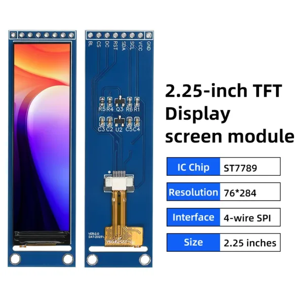 2.25-inch TFT LCD Small Screen Module ST7789 Screen 76*284 Module Full Viewing Angle SPI Color Screen 8-pin Blue Board Module
$6.90 – $7.90Price range: $6.90 through $7.90
2.25-inch TFT LCD Small Screen Module ST7789 Screen 76*284 Module Full Viewing Angle SPI Color Screen 8-pin Blue Board Module
$6.90 – $7.90Price range: $6.90 through $7.90
 Meshtastic Node Wio Tracker L1 LoRa Wio-SX1262 862-930MHz 868MHz 915MHz NRF52840 L76K GPS,Wireless, Low-power, Development Board
$35.90 – $54.90Price range: $35.90 through $54.90
Meshtastic Node Wio Tracker L1 LoRa Wio-SX1262 862-930MHz 868MHz 915MHz NRF52840 L76K GPS,Wireless, Low-power, Development Board
$35.90 – $54.90Price range: $35.90 through $54.90
The nRF52840 is one of the most popular BLE and multiprotocol chips in the world, and for good reason: it
The ESP32-C6 looks, at first glance, like a small update to the ESP32 family. It has more radios, a newer
Most teams frame this as a salary-versus-invoice decision. A layout engineer costs a certain amount per year; a layout shop
Choosing a PCB design service for an IoT product is harder than choosing one for a simple board, because an
If you have ever asked three layout shops for a quote on the same board and gotten three wildly different
Most people who approach a PCB design firm for the first time are not asking for a datasheet. They are
No account yet?
Create an Account