In high-reliability electronics, particularly automotive applications, a PCB layout is not merely an exercise in electrical connectivity. It is the foundational blueprint for manufacturing feasibility. A schematic that functions perfectly in simulation can still result in catastrophic assembly failures if it ignores the physical realities of solder paste rheology, pick-and-place mechanics, and reflow thermodynamics.
This document distills critical Design for Manufacturability (DFM) and Design for Assembly (DFA) standards specifically tailored for automotive and high-reliability SMT/DIP processes. It serves as a rigorous validation framework to ensure your design survives the demands of mass production without costly respins.
1. Core Layout and Panelization Architecture
The physical structure of the PCB dictates the efficiency and yield of the entire SMT line. Adhering to strict panelization rules is the first line of defense against assembly defects.
- Component Orientation: When the PCB enters the reflow oven, the long axis of surface-mount components must be perpendicular to the conveyor direction. This minimizes the risk of component drift or tombstoning caused by asymmetric surface tension during solder melting.
- Keep-Out Zones:
- Maintain a strict 3mm to 5mm keep-out zone around all BGA packages to ensure accessibility for X-ray inspection and rework.
- Keep SMD components at least 3mm away from board edges, connectors, and depaneling routes (mouse bites or V-cuts) to prevent mechanical stress damage during insertion or board separation.
- Double-Sided Reflow Constraints: For boards undergoing double-sided reflow, heavy or large components must be placed on the primary (top) side. If placement on the bottom is unavoidable, component weight-to-pad-area ratios must be strictly validated (e.g., chip devices ≤0.075g/mm², J-leaded devices ≤0.200g/mm²) to prevent gravitational drop-out during the second pass.
- Panelization and Process Edges:
- Panel dimensions should ideally fall between 100x50mm and 300x250mm.
- Process edges (breakaway tabs) must be ≥8mm in the conveyor direction and ≥3mm perpendicularly.
- Use mouse-bite perforations for depaneling (2.0mm hole diameter, 1.2mm web thickness). Crucially, these perforations must not be plated (no copper in the holes) to prevent tearing and tool damage during automated depaneling.
- All panel corners must feature an R5mm chamfer to prevent jamming in SMT conveyor tracks.
2. Fiducial Marks and Optical Alignment
Precise machine vision is non-negotiable for high-speed placement, especially for fine-pitch automotive components.
- Specification: Global and local fiducial marks must be circular pads with a diameter of exactly 1.0mm.
- Clearance: A 2.0mm radius around the fiducial must be completely free of solder mask (bare copper) and surrounded by a protective copper ring to prevent oxidation and ensure high-contrast optical recognition.
- Placement: A minimum of three non-collinear fiducials is required per panel. They must be placed diagonally and must not be centrally symmetric (the distance difference to the board edge must be >5mm) to prevent the pick-and-place machine from misidentifying board orientation (e.g., loading the board upside down).
3. Component-Specific DFM Rules
Different package families present unique manufacturing challenges. Layouts must be optimized for soldering, inspection, and mechanical reliability.
- BGA and QFN/SON:
- Vias must never be placed directly inside the solder pad. If thermal vias are required under the exposed thermal pad, they must be ≤8mil in diameter and either resin-filled and capped or back-drilled to prevent solder wicking and voiding.
- Traces exiting BGA pads must not expose bare copper on the sides, which can cause solder bridging.
- Chip Components (0402 and larger):
- Avoid connecting logically linked pads of small capacitors/resistors to large, unbroken copper pours. This creates severe thermal imbalance during reflow, leading to tombstoning. Use thermal reliefs (cross-hatched connections) for pads connected to ground planes.
- Maintain a minimum spacing of ≥0.3mm between identical components and ≥0.13*h + 0.3mm between different components (where h is the height difference).
- Connectors and Through-Hole (THT) Components:
- For press-fit or wave-soldered connectors, ensure the PCB mounting hole diameter is 0.15–0.2mm larger than the component's positioning pin to accommodate placement tolerance without interference.
- THT component leads should protrude 1.0–1.5mm (max 2.5mm) beyond the PCB surface to ensure reliable wave soldering without mechanical interference.
- Pick-and-Place Clearance: Components like USB, HDMI, and SD card sockets must feature a flat, unobstructed top surface (e.g., >8x8mm for large connectors) to allow the vacuum nozzle to securely grip the component during high-speed placement.
4. Silkscreen and Assembly Validation
Silkscreen is not just for aesthetics; it is a critical tool for assembly verification, debugging, and traceability.
- Polarity and Orientation: All polarized components (diodes, tantalum capacitors, ICs) must have a clear, unambiguous Pin 1 indicator. This silkscreen must never be placed underneath the component body where it would be hidden after assembly.
- Barcode Traceability: Allocate a dedicated 15x15mm area with a white, hollow silkscreen box for barcode printing. This area must be on a solid copper pour covered by solder mask, isolated from surrounding traces, to ensure reliable automated scanning.
- Solder Mask Definition: For fine-pitch ICs (e.g., power amplifiers), apply solder mask dams between adjacent pads to prevent solder bridging during reflow.
5. The High Cost of Poor Layout and How to Mitigate It
A layout that ignores DFM rules inevitably leads to prototype failures: tombstoning 0402 capacitors, head-in-pillow defects on BGAs, or cold joints on thermal pads. Iterating through multiple board spins to fix these issues drains R&D budgets and delays time-to-market.
To eliminate the financial friction of physical validation, we maintain a strategic prototyping initiative: $2 for 5 pieces for custom PCB under 50mm x 50mm. You can order these directly via our streamlined online ordering platform.
Hardware engineers can use this program to fabricate dedicated DFM test coupons. This allows you to empirically verify solder paste release on fine-pitch pads, test the mechanical integrity of your depaneling routes, and validate thermal relief effectiveness before committing to expensive, full-scale production tooling.
6. Professional Support for High-Reliability Designs
Achieving automotive-grade reliability requires more than just a checklist; it requires deep expertise in stack-up design, impedance control, and advanced DFM rules. If your team lacks the bandwidth or specialized knowledge to optimize complex layouts, our professional PCB Layout and Design services are available. Our engineers design with manufacturing in mind from day one, ensuring your Gerber files are optimized for yield.
Furthermore, precise solder paste deposition is critical for the fine-pitch components discussed above. We provide high-precision SMT stencils with optimized aperture designs (such as step-stencils or nano-coated options) to ensure consistent paste volume and prevent bridging.
When your design is validated and you are ready to scale, initiating an OEM/ODM bulk manufacturing inquiry allows our process engineering team to integrate your specific DFM requirements into our high-volume Statistical Process Control (SPC) monitoring, ensuring consistent, audit-ready quality across every production batch.
For any specific technical questions regarding your stack-up, DFM requirements, or component sourcing, please contact us to speak directly with our engineering team.
FAQ
Q: Why must mouse-bite depaneling holes be left unplated (no copper)?
A: If the perforation holes are plated, the copper creates a continuous, strong mechanical bond between the panels. During automated depaneling, this can cause the router bit or blade to tear the PCB substrate, generating excessive dust that can contaminate nearby components or cause micro-shorts.
Q: How does connecting a small chip component to a large copper pour cause tombstoning?
A: Large copper areas act as heat sinks, drawing heat away from the pad during reflow. If one pad of a small component is on a large pour and the other is not, the temperature differential causes uneven solder melting. The surface tension of the molten solder on the hotter pad pulls the component upright, resulting in a tombstone defect.
Q: What is the minimum keep-out distance for a BGA package?
A: A minimum of 3mm to 5mm of clear space is required around all sides of a BGA. This ensures that rework tools can access the component for removal and that X-ray inspection equipment can clearly image the solder joints without obstruction from adjacent components.
Q: Why is central symmetry forbidden for fiducial mark placement?
A: If fiducial marks are placed in a perfectly symmetrical pattern (e.g., a perfect rectangle in the center of the board), the pick-and-place machine's vision system may not be able to distinguish the board's correct orientation. This can result in the board being loaded upside down or rotated 180 degrees, causing catastrophic placement errors.
Robust PCBA design is the intersection of electrical engineering and manufacturing science. By strictly adhering to these automotive-grade DFM and DFA guidelines, you can eliminate the most common causes of assembly failure, reduce prototyping cycles, and ensure long-term field reliability.

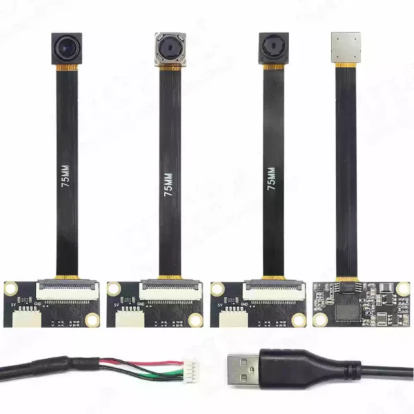 OV5693 USB Camera Module – 5MP (2952 x 1944), 1080P, Autofocus
$15.90
OV5693 USB Camera Module – 5MP (2952 x 1944), 1080P, Autofocus
$15.90
 GPIO Headers Expansion Board HAT for RPI RasPi Raspberry Pi PICO 2 W RP2350 Breakout Shield Breadboard Microcontroller Projects
 9.7 Inch Black White Epaper Display
$60.00
9.7 Inch Black White Epaper Display
$60.00
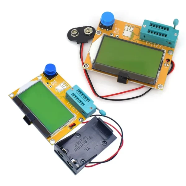 LCR-T4 T3 ESR Meter Transistor Tester Diode Triode Capacitance SCR Inductance MOS PNP NPN
$1.90 – $8.90Price range: $1.90 through $8.90
LCR-T4 T3 ESR Meter Transistor Tester Diode Triode Capacitance SCR Inductance MOS PNP NPN
$1.90 – $8.90Price range: $1.90 through $8.90
 L60A Interactive Cat Chase Run Exercise Adjustable Speed Kitten For Bored Cats Mental Stimulation Cat Treadmill
$47.90
L60A Interactive Cat Chase Run Exercise Adjustable Speed Kitten For Bored Cats Mental Stimulation Cat Treadmill
$47.90