
The 5 Most Common Layout Mistakes We Fix in Client Boards
We review a lot of boards — some designed in-house, some by other contractors, some by founders doing their own
EMC testing is expensive, and failing it is worse than the test fee — it costs you a respin, a schedule slip, and a second trip to the lab. The frustrating part is that the majority of EMC failures are not caused by exotic physics. They are caused by layout decisions that could have been made correctly the first time, by applying a checklist before the board was fabricated.
This is that checklist. It is organized around the things that actually cause most EMC failures on real boards, with a focus on what you can check without a lab.
EMI is rarely about the signal you intended to send. It is about the return current that came along for the ride, and the loop areas those currents flow in. Every current has a return path, and if that path is not the one directly beneath the trace, the resulting loop acts as an antenna. Large, poorly controlled loops radiate; small, tight loops do not.
With that in mind, the checklist is mostly about controlling return paths and isolating the noisy parts of the design from the sensitive parts.
This is the foundation. Get it right and most other problems shrink.
Keep noise sources and sensitive circuits physically apart.
Interfaces are where emissions enter and leave the board, so they get special attention.
Fast edges are the source of most emissions.
Noise on the power rails couples into everything.
EMC is not only the board.
You do not need a full lab to catch many problems. If you have any access to a spectrum analyzer and a near-field probe, a pre-scan can find the worst offenders before you pay for formal testing. Even a rough scan identifies the frequencies where your board is loudest, which tells you which part of the design to fix.
For products with radios, pre-test the antenna performance in the real enclosure. The antenna's behavior changes once it is in the product, and finding that out at the certification lab is expensive.
If a board does fail, the fix is almost always one of these: improve the return path, tighten a loop area, add or relocate filtering, slow an edge, or improve grounding. Work from the loudest frequency back to its source. In our experience, the majority of failures trace to one or two specific decisions, not a globally bad design.
The good news is that the same checklist that prevents failures also guides the fixes, because the mechanisms are the same.
If your product is going to a regulated market, involve EMC thinking at the layout stage, not after. The design decisions that make certification easy or hard are made in the layout, and retrofitting them onto a finished board is far more expensive than building them in. A board designed with these questions in mind usually passes with minor adjustments; a board designed without them often needs a respin.
Most EMC failures are decided in the layout. The main mechanism is uncontrolled return current and large loop areas, so the checklist centers on continuous reference planes, return vias, and tight loops. Group noisy circuits away from sensitive ones, filter and protect at every interface, slow unnecessarily fast edges at the driver, keep switching loops small, and place decoupling properly. Pre-test if you can, especially antenna performance in the real enclosure.
And involve EMC thinking at the layout stage, because that is where certification is won or lost.
We lay out boards with EMC and certification in mind from the first placement, rather than treating it as a post-fabrication problem.
If your product has a certification target, that should shape the layout from day one, and that is how we work: pcb-layout for layout, pcb-design for full design from schematic to Gerbers, and PCB PCBA order online when it is time to build.
Tell us your certification target and we will design toward it, not around it.
 6-inch Replacement LCD screen for Kindle 3 KINDLE KEYBOARD 3G ED060SC7 D000901
$18.90
6-inch Replacement LCD screen for Kindle 3 KINDLE KEYBOARD 3G ED060SC7 D000901
$18.90
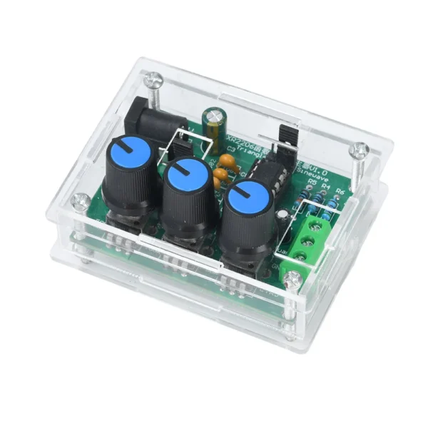 DC 9-12V High Precision Signal Generator DIY Kit Sine Triangle Square Waves 1Hz 1MHz Frequency Range Adjustable Frequency
$4.50 – $5.00Price range: $4.50 through $5.00
DC 9-12V High Precision Signal Generator DIY Kit Sine Triangle Square Waves 1Hz 1MHz Frequency Range Adjustable Frequency
$4.50 – $5.00Price range: $4.50 through $5.00
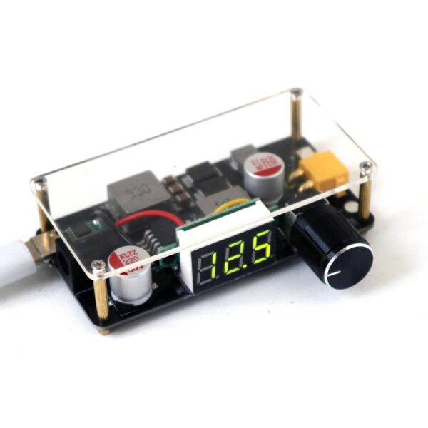 Desktop Adjustable Buck-Boost Power Supply Type-C USB PD DC 5-35V to 1.25-36V (3.3V/5V/12V/15V/24V) Voltage Converter with Di
$16.90
Desktop Adjustable Buck-Boost Power Supply Type-C USB PD DC 5-35V to 1.25-36V (3.3V/5V/12V/15V/24V) Voltage Converter with Di
$16.90
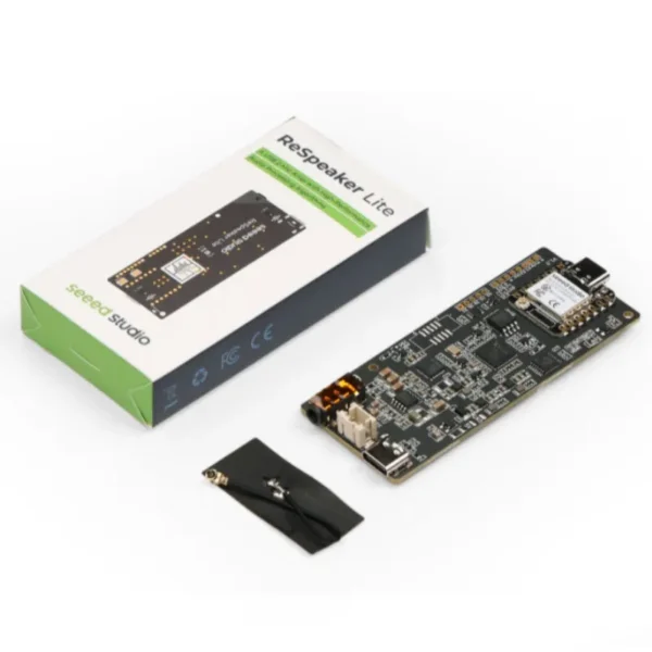 ReSpeaker Lite Voice Assistant Kit, ESPHome Assistant, 2 Mic Array with XIAO ESP32S3 pre-soldered, Mono Enclosed Speaker
$40.90 – $49.80Price range: $40.90 through $49.80
ReSpeaker Lite Voice Assistant Kit, ESPHome Assistant, 2 Mic Array with XIAO ESP32S3 pre-soldered, Mono Enclosed Speaker
$40.90 – $49.80Price range: $40.90 through $49.80
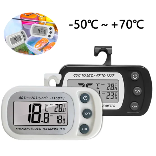 Fridge Thermometer With Hook Anti-Humidity Refrigerator Freezer Electric Digital Thermometer Temperature Monitor LCD Display
$1.90
Fridge Thermometer With Hook Anti-Humidity Refrigerator Freezer Electric Digital Thermometer Temperature Monitor LCD Display
$1.90
We review a lot of boards — some designed in-house, some by other contractors, some by founders doing their own
When a battery-powered product dies too soon, the instinct is to blame the firmware. Surely there is a sleep mode
A wearable PCB is not just a small PCB. It is a board where every constraint that normally has some
The STM32 family is the workhorse of embedded hardware, and almost every project that uses one starts the same way:
The nRF52840 is one of the most popular BLE and multiprotocol chips in the world, and for good reason: it
The ESP32-C6 looks, at first glance, like a small update to the ESP32 family. It has more radios, a newer
No account yet?
Create an Account