
EMC/EMI Checklist Before Your Board Goes to Certification
EMC testing is expensive, and failing it is worse than the test fee — it costs you a respin, a
A wearable PCB is not just a small PCB. It is a board where every constraint that normally has some slack has none. There is no room to move the antenna. There is no spare current. There is no extra layer you can add without changing the mechanical fit. And the board has to survive being worn — against skin, through sweat, and across the temperature swings of daily life.
Designing a wearable means accepting these constraints up front and designing around them, rather than discovering them after the third respin. Here is how to think about it.
On most projects, the schematic comes first and the board grows to fit it. In wearables, it is the opposite. The product's shape — a ring, a watch case, a patch, a band — defines the board outline, and the electronics have to fit inside that. The board size is not negotiable; it is given.
This changes the design order. You have to plan component placement against a fixed outline from the very beginning, and you have to be willing to change the schematic to fit the board rather than the other way around. A component that "would be nice" but does not fit is simply not on the board.
Practical approach: start with a board outline and a rigid-flex or rigid strategy, lay out the largest components first (the battery, the module, the display, the connector), and route what remains. Accept from the start that the schematic will be trimmed to fit.
Most wearables are wireless, which means you have a 2.4 GHz radio — BLE, Wi-Fi, or both — sitting inside a board smaller than a thumbnail. Antenna design in this space is the hardest part of the project.
Your options, roughly in order of difficulty:
The uncomfortable truth about wearables and antennas is that the ground plane the antenna needs is often the very thing the product does not provide. Design the antenna around the actual, limited ground you have — and test the real assembly, because the enclosure and the body nearby will change the tuning.
A wearable runs on a tiny battery, often a coin cell or a small lithium cell, and it has to last days, weeks, or months. Sleep current is not a detail; it is the product.
Layout decisions that decide battery life:
A wearable that works on the bench and dies in three days is almost always a sleep-current problem, and it is decided in the layout and component choices, not the firmware alone.
Many wearables use flex or rigid-flex boards to fit a curved product. This is a different design discipline:
If your wearable includes a curved surface, rigid-flex is often the only way to fit electronics into it, and it changes the layout rules accordingly.
A wearable is exposed to skin, sweat, and motion. That affects both the mechanical design and the materials:
These are not layout rules in the classical sense, but they influence the layout, because the protective measures take space and the thermal path follows the copper.
Given all of the above, a practical sequence:
The last point is where wearables differ most from other products: the antenna behaves differently once the enclosure and the wearer are involved. Plan to test the actual assembly.
We layout compact, RF-bearing boards, including wearable-class designs where the antenna and the power budget are the hard constraints. If you are trying to fit a wireless product into a very small space, that is our kind of problem: pcb-layout. For the full design path from schematic to Gerbers, see pcb-design.
Fabrication and assembly of the resulting boards run through PCB PCBA order online.
Send us your enclosure outline and we will tell you honestly whether the electronics fit, and where the compromises will be.
Wearable PCB design is defined by constraints that have no slack: a fixed, tiny outline; a 2.4 GHz antenna with almost no ground plane; a battery measured in microamps of sleep current; and a board that gets worn. Fix the outline first and let the schematic shrink to fit. Choose the antenna based on the ground you actually have, and test the real assembly. Design power around sleep current, not active current.
If the product curves, plan for flex or rigid-flex from the start. And remember the board will be worn, so protect it and think about thermal paths.
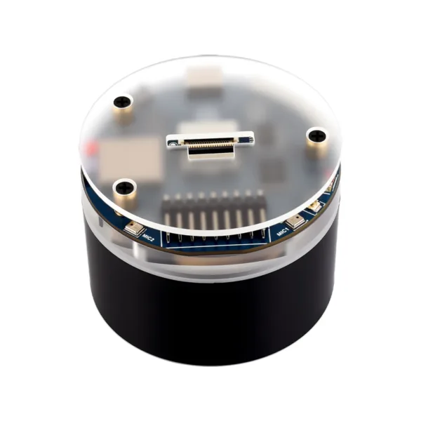 Waveshare ESP32-S3 AI Smart Speaker Development Board, Onboard Dual Digital Microphone Array, Supports Noise Reduction
 Banana Pi OpenWrt One MediaTek MT7981B 1GB DDR4 2.5GbE RJ45 and Gigabit Ethernet RJ45 256 MiB SPI NAND Open Source Smart Router
$290.80
Banana Pi OpenWrt One MediaTek MT7981B 1GB DDR4 2.5GbE RJ45 and Gigabit Ethernet RJ45 256 MiB SPI NAND Open Source Smart Router
$290.80
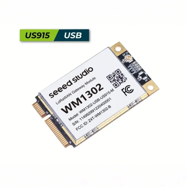 WM1302 LoRaWAN Gateway Module USB US915MHz Without SX1262
$37.90
WM1302 LoRaWAN Gateway Module USB US915MHz Without SX1262
$37.90
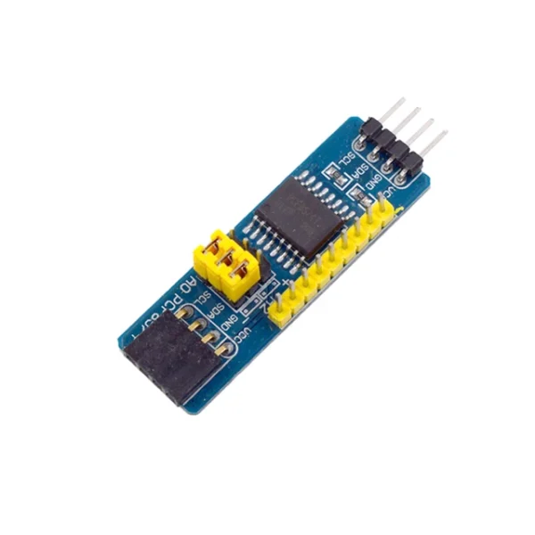 PCF8574 I2C Interface 8bit IO MCU Expansion Board I/O Expander I2C Bus Evaluation Development Module AVR STM8 C8051F For Arduino
$1.90
PCF8574 I2C Interface 8bit IO MCU Expansion Board I/O Expander I2C Bus Evaluation Development Module AVR STM8 C8051F For Arduino
$1.90
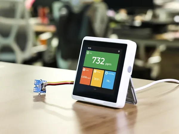 SenseCAP Indicator D1Pro, 4-Inch Touch Screen IoT development platform powered by ESP32S3 & RP2040
$179.80
SenseCAP Indicator D1Pro, 4-Inch Touch Screen IoT development platform powered by ESP32S3 & RP2040
$179.80
EMC testing is expensive, and failing it is worse than the test fee — it costs you a respin, a
We review a lot of boards — some designed in-house, some by other contractors, some by founders doing their own
When a battery-powered product dies too soon, the instinct is to blame the firmware. Surely there is a sleep mode
The STM32 family is the workhorse of embedded hardware, and almost every project that uses one starts the same way:
The nRF52840 is one of the most popular BLE and multiprotocol chips in the world, and for good reason: it
The ESP32-C6 looks, at first glance, like a small update to the ESP32 family. It has more radios, a newer
No account yet?
Create an Account