
EMC/EMI Checklist Before Your Board Goes to Certification
EMC testing is expensive, and failing it is worse than the test fee — it costs you a respin, a
The STM32 family is the workhorse of embedded hardware, and almost every project that uses one starts the same way: on a dev board. The dev board works. The firmware runs. Then the time comes to move to a custom PCB, and suddenly a design that "just worked" has to work on a board you built yourself, with none of the crutches the dev board provided.
That transition is where many first custom designs stumble. Not because the STM32 is hard, but because the dev board quietly handled a dozen things that a bare chip does not. Here is what changes, and how to plan for it.
If you look carefully at an STM32 dev board, you will find it contains not just the MCU but a complete support system. When you go custom, you inherit all of it.
Each of these is a small design task, and skipping any of them is a common cause of a first board that does not boot.
The most common reason a first STM32 custom board fails to come up is power. Either the rail is wrong, the regulator cannot supply the required current, or the decoupling is inadequate.
A few rules that prevent most of it:
The good news: STM32 reference designs and evaluation board schematics are excellent, and copying them faithfully prevents most power mistakes.
The STM32's main clock usually comes from an external crystal or a ceramic resonator, and this is the second most common source of first-spin problems.
If you are using an internal oscillator and do not need external clock accuracy, you can skip the crystal — but be deliberate about that decision, because it affects USB and any timing-sensitive peripheral.
This sounds obvious, but it is one of the most painful mistakes in custom design: a board with no accessible SWD, or with SWD pins that conflict with something else.
A board without debug access is, at best, a board you can flash once and hope. Plan for debug on every revision.
STM32 boot mode is set by specific pins, and the wrong setting means the chip does not start the way you expect. Decide now how you intend to program the chip — SWD, UART, or USB bootloader — and configure the boot pins accordingly. Include a reset circuit; the vendor reference shows the standard approach.
If your design exposes USB, UART, or any external interface, protect it:
If you use the STM32's native USB, follow the vendor's USB layout guidance. It differs by part and by speed.
An STM32 board is usually not a high-speed board, but it is not a free-for-all either. A few habits keep you out of trouble:
For most STM32 products, a well-planned two- or four-layer board is entirely sufficient. The layer count should follow from the design, not from habit.
Two things commonly get missed in the jump to production.
Programming strategy. How will production units be programmed? A test clip, pogo pins, a programming fixture, or a pre-programmed part? This affects your layout — bring out the necessary signals and test points.
DFM and assembly. Your dev-board prototype was hand-soldered and forgiving. Production assembly has real DFM rules: component clearances, courtyard spacing, panelization. Design for the process you will actually use.
We design and lay out STM32 boards for teams moving from a working dev board to a product. If your schematic is ready and you need layout, that is pcb-layout. If you would rather hand over the whole path from schematic to Gerbers, see pcb-design. When it is time to build and assemble, PCB PCBA order online handles that step.
Send us your part number and constraints, and we will flag the power, clock, and debug risks before layout begins.
Moving an STM32 from a dev board to a custom PCB means inheriting everything the dev board did for you: power regulation, clocking, reset and boot configuration, debug access, decoupling, and USB. Power and clocking are where first boards fail most often — copy the vendor reference designs faithfully. Always bring out SWD and reset. Configure boot pins for how you will actually program the chip. Plan your production programming and DFM before you route.
A well-planned two- or four-layer board is enough for most STM32 designs.
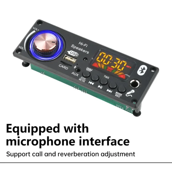 DC12V MP3 Bluetooth Decoder Board BT5.3 Amplifier Car Audio DIY Music Player FM Radio Module RGB TF AUX USB Mic Record WAV APE
$5.50 – $5.70Price range: $5.50 through $5.70
DC12V MP3 Bluetooth Decoder Board BT5.3 Amplifier Car Audio DIY Music Player FM Radio Module RGB TF AUX USB Mic Record WAV APE
$5.50 – $5.70Price range: $5.50 through $5.70
 Grove - Temperature & Humidity Sensor(DHT11)
$8.90
Grove - Temperature & Humidity Sensor(DHT11)
$8.90
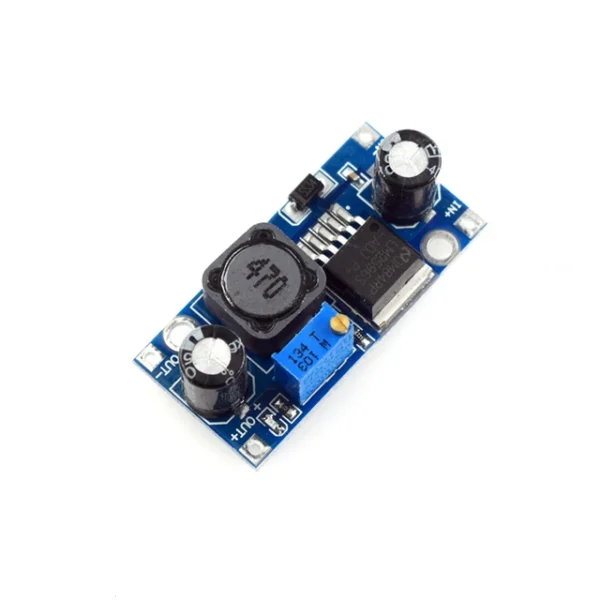 LM2596S DC-DC 3A 92% Step-down Power Supply Module Adjustable Step-down module 3.2V-35V To 1.25V-30V Voltage Regulator
$2.50
LM2596S DC-DC 3A 92% Step-down Power Supply Module Adjustable Step-down module 3.2V-35V To 1.25V-30V Voltage Regulator
$2.50
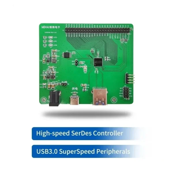 CH569 development board USB3.0 Super-Speed Interface MCU Gigabit Ethernet PHY HSPI CH569W-EVT Evaluation Board New Original
$33.90
CH569 development board USB3.0 Super-Speed Interface MCU Gigabit Ethernet PHY HSPI CH569W-EVT Evaluation Board New Original
$33.90
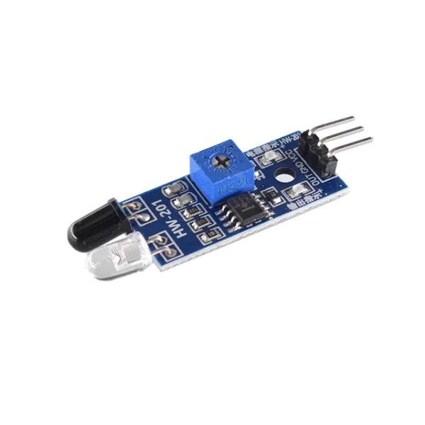 IR Infrared Reflectance Sensor Obstacle Avoidance Module Tracing Sensor Tracing Module For Arduino Diy Smart Car Robot
$1.90
IR Infrared Reflectance Sensor Obstacle Avoidance Module Tracing Sensor Tracing Module For Arduino Diy Smart Car Robot
$1.90
EMC testing is expensive, and failing it is worse than the test fee — it costs you a respin, a
We review a lot of boards — some designed in-house, some by other contractors, some by founders doing their own
When a battery-powered product dies too soon, the instinct is to blame the firmware. Surely there is a sleep mode
A wearable PCB is not just a small PCB. It is a board where every constraint that normally has some
The nRF52840 is one of the most popular BLE and multiprotocol chips in the world, and for good reason: it
The ESP32-C6 looks, at first glance, like a small update to the ESP32 family. It has more radios, a newer
No account yet?
Create an Account