
ESP32-C6 Layout Guide: What's Different from the Classic ESP32
The ESP32-C6 looks, at first glance, like a small update to the ESP32 family. It has more radios, a newer
The nRF52840 is one of the most popular BLE and multiprotocol chips in the world, and for good reason: it is well-documented, well-supported, and proven in products from wearables to industrial sensors. But popularity is not the same as forgiving. The 52840 is a 2.4 GHz radio, and the layout around that radio decides whether your product reaches across a room or across a building.
This guide covers what actually matters in an nRF52840 layout: the antenna, the matching network, the feedline, the power design, and the certification consequences of each.
Everything about BLE range, reliability, and connection stability traces back to the antenna and the board around it. On an nRF52840 design you have three broad choices, and each has layout consequences.
Chip antenna. Small, cheap, and adequate for many products, but sensitive to the ground plane size and clearance. A chip antenna that is starved of clearance underperforms its datasheet badly.
PCB trace antenna. Free in BOM terms and popular for compact products, but it must be copied faithfully from a reference design. Improvised PCB antennas rarely work.
External antenna (via connector or module). Best performance and easiest certification if you use a pre-certified module, but adds cost and a connector.
Whichever you choose, the keep-out rules are similar: no copper in the antenna region, a continuous ground plane as the antenna's reference, and real physical clearance from metal, batteries, and enclosure walls.
For the nRF52840, the most common range killer is a board that is too small. If your PCB is barely larger than the chip, the ground plane the antenna needs simply is not there. In that case, an external antenna or a module with a certified antenna is the honest answer.
Between the radio output and the antenna sits a matching network — typically a pi-network of a few components. This network transforms the chip's output impedance to 50 ohms and tunes the antenna.
The rules here are simple and strict:
The most common matching mistake is placing the components correctly but routing them with long, thin traces. At 2.4 GHz, a few millimeters of trace is electrically significant. Short and direct is the rule.
The feedline is the trace between the matching network and the antenna. It must present a 50 ohm impedance, which means its width, its dielectric, and its reference plane all have to be controlled.
For a typical two-layer board, the feedline is usually a coplanar waveguide with ground, where the trace width and the gap to the surrounding ground set the impedance. For a four-layer board, a microstrip over a solid ground plane is more common. Either way, the impedance is a function of geometry, and the fabricator's stackup determines the exact dimensions.
Two practical points:
Do not run the feedline near switching supplies, crystals, or high-speed digital traces. Coupling onto the feedline degrades the radio without any obvious symptom until you test range.
The nRF52840 needs a clean ground reference for both the radio and the digital core. The rules are familiar but worth repeating:
If you are using a module (like a certified nRF52840 module), the module vendor's reference layout and keep-out are authoritative. Follow them exactly — the certification depends on it.
Many nRF52840 products are battery-powered, and here the power design is inseparable from the layout.
Because BLE products spend most of their life asleep, the sleep current often determines battery life more than the transmit current. Layout choices — component selection, leakage, regulator quiescent current — are where that battle is won or lost.
The nRF52840 supports both an internal LDO and a DC/DC converter, and the way you configure and lay out power affects both efficiency and RF performance. The DC/DC requires specific inductors and capacitors placed per the reference design. Do not improvise the power topology; the radio performance depends on it.
Also keep the high-voltage mode and regulator configuration consistent with your firmware. A layout that assumes one mode and firmware that uses another is a common source of confusing bring-up problems.
The nRF52840 comes in both chip and module forms, and the certification path depends on which you use.
With a pre-certified module, most of the radio certification burden transfers to the module vendor — but only if you follow the module's integration requirements to the letter. That means exact keep-out, no changes to the matching network, and the module's approved antenna. Modify any of that and you take the certification burden back.
With a chip-down design, you own the radio certification work: conducted and radiated testing, and any regional approvals. This is entirely doable, but it has to be designed for from the start. The layout decisions above are what make certification straightforward or painful.
Design to your certification target from day one, and pick module or chip-down partly on how much certification work you want to own.
We lay out nRF52840 and other 2.4 GHz designs for clients who need the RF section done right the first time. If you want your antenna, matching, and power handled by people who do this daily, that is our layout service. For schematic-to-Gerbers design, see pcb-design.
Board fabrication and assembly run through PCB PCBA order online.
Send us your antenna choice and constraints, and we will tell you where the certification risk sits.
On an nRF52840 layout, the antenna, the matching network, and the 50 ohm feedline decide your range. Do not improvise any of them — copy from reference designs, place matching components immediately at the chip, and specify controlled impedance with your fabricator. Keep the ground continuous under the entire RF path and stitch generously. For battery products, sleep current is decided by the power layout, not the radio.
Whether you use a module or go chip-down determines who owns certification, and that choice has to be built into the layout from the start.
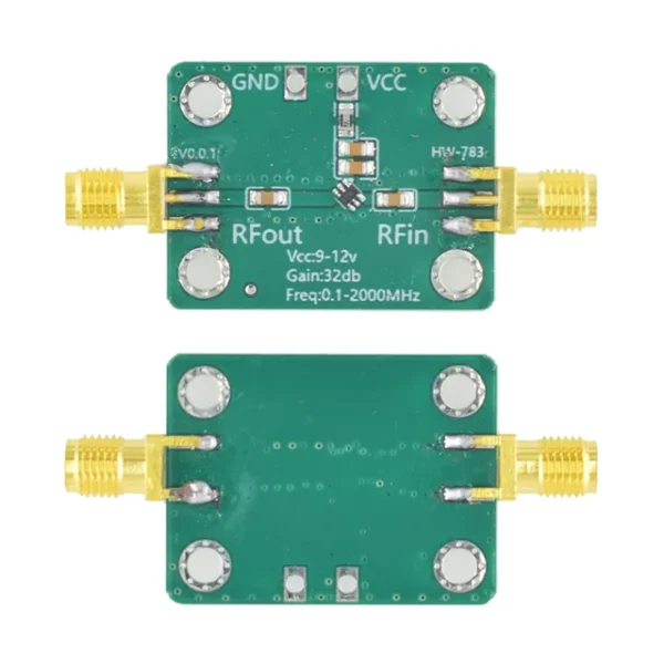 0.1MHz-2000MHz 32dB LNA RF Broadband Low Noise Amplifier Module Radio Frequency Wideband Amplifier
$4.90
0.1MHz-2000MHz 32dB LNA RF Broadband Low Noise Amplifier Module Radio Frequency Wideband Amplifier
$4.90
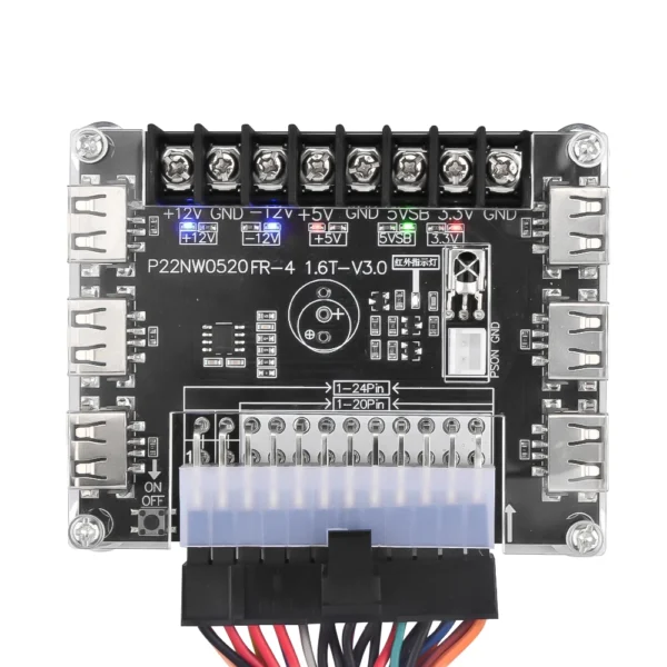 24 Pins ATX Power Supply Breakout Board and Acrylic Case Kit Module Adapter Power Connector Support 12V -12V 5V 5VSB 3.3V
$6.90 – $7.50Price range: $6.90 through $7.50
24 Pins ATX Power Supply Breakout Board and Acrylic Case Kit Module Adapter Power Connector Support 12V -12V 5V 5VSB 3.3V
$6.90 – $7.50Price range: $6.90 through $7.50
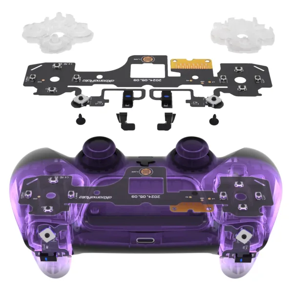 eXtremeRate Whole Clicky Kit V2 for ps5 Controller BDM-040/050 Shoulder Face Dpad Buttons, Micro Switch Clicky Hair Trigger Kit
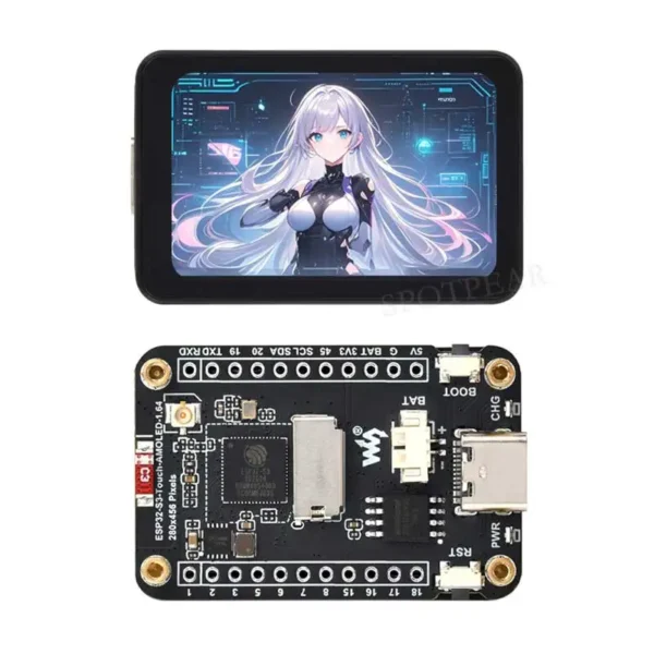 ESP32 S3 Development Board 1.64inch AMOLED Display 1.64 inch TouchScreen For Arduino LVGL With SD-Port/ QMI8658C 6-Axis Sensor
$28.90
ESP32 S3 Development Board 1.64inch AMOLED Display 1.64 inch TouchScreen For Arduino LVGL With SD-Port/ QMI8658C 6-Axis Sensor
$28.90
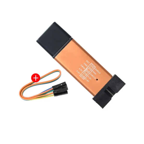 1Set ST LINK Stlink ST-Link V2 Mini STM8 STM32 Simulator Download Programmer Programming With Cover DuPont Cable ST Link V2
$3.90
1Set ST LINK Stlink ST-Link V2 Mini STM8 STM32 Simulator Download Programmer Programming With Cover DuPont Cable ST Link V2
$3.90
The ESP32-C6 looks, at first glance, like a small update to the ESP32 family. It has more radios, a newer
Most teams frame this as a salary-versus-invoice decision. A layout engineer costs a certain amount per year; a layout shop
Choosing a PCB design service for an IoT product is harder than choosing one for a simple board, because an
If you have ever asked three layout shops for a quote on the same board and gotten three wildly different
Your firmware works. The serial log prints clean, the sensor reads true, and the board boots every time. Then you
Most people who approach a PCB design firm for the first time are not asking for a datasheet. They are
No account yet?
Create an Account