
EMC/EMI Checklist Before Your Board Goes to Certification
EMC testing is expensive, and failing it is worse than the test fee — it costs you a respin, a
You finish the schematic, place the USB-C connector, route the two data lines side by side, and ship the board. The device enumerates on your bench. Then a customer plugs it into a laptop, and it shows up as an unknown device — or works on one cable and not another. Nothing in the schematic changed. The problem is in the copper.
USB is the interface your customers touch first. It is also the one that punishes layout mistakes most quietly, because a marginal differential pair often works on the bench and fails in the field. This guide covers what actually matters when routing USB 2.0 High-Speed and USB-C on an ESP32-S3 board, and where designs most often go wrong.
USB 2.0 High-Speed uses a differential pair with a target differential impedance of 90Ω, with a tolerance of plus or minus 10 percent. The number is not arbitrary: it is the impedance the transceiver expects, and deviation causes reflections that eat into signal integrity.
The trap is treating 90Ω as a fixed trace width. It is not. Differential impedance depends on the trace width, the gap between the two traces, the dielectric thickness to the reference plane, and the copper weight. Change your stackup and the same geometry is no longer 90Ω. Every fabricator's impedance calculator will give you a different answer for the same nominal width, because the dielectric constant and prepreg thickness differ.
The practical rule: define your stackup first, then get the trace geometry from your fabricator's calculator for that exact stackup, and recheck it if anything in the stackup changes.
The D+ and D- traces should be routed as a pair, at equal length, in parallel. Length matching keeps the two signals' propagation delay aligned so the differential receiver sees a clean difference signal.
Two things get overdone here. First, people chase sub-millimetre matching when the real requirement is much looser — the ESP32-S3 USB PHY tolerates a reasonable amount of skew. Second, people add serpentine meanders to force perfect equality and accidentally create impedance discontinuities, which is worse than the small skew they were trying to remove. Match within your device's guideline, use gentle serpentine if you must, and stop.
Every differential pair needs a continuous reference plane directly beneath it. On a four-layer stackup, that is usually the ground layer. On a two-layer board, it is harder, and USB is one of the reasons two-layer designs struggle at High-Speed.
The failure mode is a pair that crosses a plane split — the return current has to take a long, looping path, and the impedance changes abruptly at the crossing. The signal reflects. The eye diagram closes. Very often this is why a board "works on some cables."
Route the pair over unbroken ground, and keep the plane continuous from connector to chip.
Every via in a differential pair is an impedance discontinuity, so the goal is to use as few as possible. When a layer transition is genuinely unavoidable, add a pair of ground return vias next to the signal vias — a ground via beside each signal via, tied to the reference plane the pair is transitioning between.
Without return vias, the return current has no short path to follow through the transition, and the discontinuity is larger than it needs to be. This one habit separates pairs that survive layer changes from pairs that do not.
Surround the USB traces with ground copper and stitch it with vias. This is not decoration: it gives the pair a stable local reference environment and reduces coupling to neighbouring signals. It also matters near the connector, where EMI is most likely to leak in or out.
Keep the traces away from the crystal, switching regulators, and the RF section. The ESP32-S3 radio and the USB PHY share a die, and coupling between them is a real path for degraded performance on both sides.
USB-C is exposed to the outside world, which means it will see electrostatic discharge. Add ESD protection close to the connector, on the data lines, with a short, direct path to ground. A protection diode placed far from the connector with a long thin ground trace does not protect anything.
Place the series resistors and the components the reference design calls for close to the chip side, as Espressif's USB layout guidance recommends. Keep the connector-to-chip path as short as your mechanics allow, because every millimetre of length is another chance to accumulate loss and mismatch.
USB layout is one of those tasks where the cost of getting it wrong is invisible until units are in customers' hands — the returns rate, the support load, the reputation. If your product relies on a reliable USB interface and you would rather not find out at the field-test stage, this is work we do routinely.
Our PCB layout service takes your schematic and mechanical constraints and returns a production-ready layout, with differential pairs, reference planes, and return paths treated as first-class constraints rather than cleanup. If your circuit is not finalized yet, our ESP32 PCB Design service covers module selection, power architecture, and connector definition before layout begins.
When the design is ready, our online PCB and PCBA ordering handles fabrication and assembly — including controlled impedance, which you should select for any board with a USB High-Speed pair, since it ensures your specified stackup is actually what gets built.
90Ω is a property of your stackup, not a trace width. Define the stackup, source the geometry from the fabricator, route a parallel length-matched pair over continuous ground, minimize vias and add return vias when you cannot, protect the connector, and keep USB clear of the noise sources. Do that and the interface stops being the thing that comes back from the field.
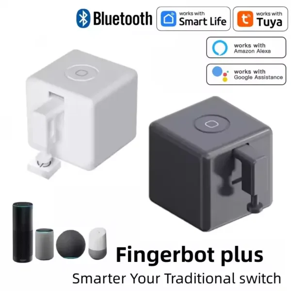 Smart Bluetooth Fingerbot - Wireless Switch Button Pusher for Smart Home, Voice Control via Alexa & Google Assistant
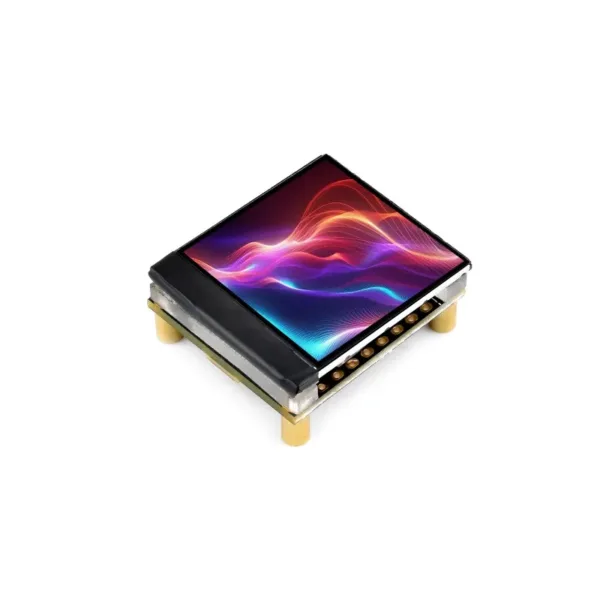 ESP32-S3 1.3inch Display Development Board, 240×240 Pixels, Built-in ST7789V2 Chip And 6-Axis IMU, 262K Color, SPI Communication
$15.90 – $29.80Price range: $15.90 through $29.80
ESP32-S3 1.3inch Display Development Board, 240×240 Pixels, Built-in ST7789V2 Chip And 6-Axis IMU, 262K Color, SPI Communication
$15.90 – $29.80Price range: $15.90 through $29.80
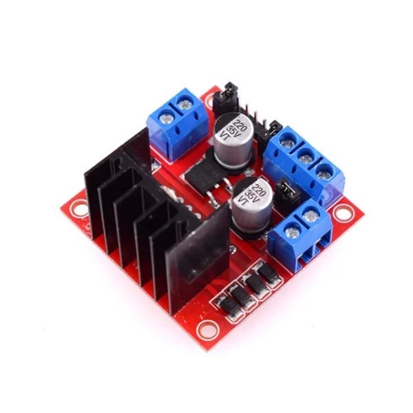 L298N Driver Board Module L298 Stepper Motor Smart Car Robot Breadboard Peltier High Power
$2.20
L298N Driver Board Module L298 Stepper Motor Smart Car Robot Breadboard Peltier High Power
$2.20
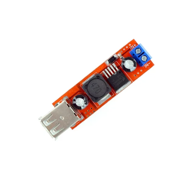 DC 6V-40V To 5V 3A Double USB Charge DC-DC Step-down Converter Module For Vehicle Charger LM2596 Dual USB
$2.90
DC 6V-40V To 5V 3A Double USB Charge DC-DC Step-down Converter Module For Vehicle Charger LM2596 Dual USB
$2.90
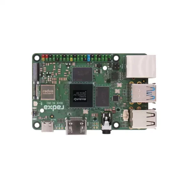 Radxa ROCK 5C RK3588S2/RK3582 SBC – Raspberry Pi 5 Alternative
$116.80 – $240.90Price range: $116.80 through $240.90
Radxa ROCK 5C RK3588S2/RK3582 SBC – Raspberry Pi 5 Alternative
$116.80 – $240.90Price range: $116.80 through $240.90
EMC testing is expensive, and failing it is worse than the test fee — it costs you a respin, a
We review a lot of boards — some designed in-house, some by other contractors, some by founders doing their own
When a battery-powered product dies too soon, the instinct is to blame the firmware. Surely there is a sleep mode
A wearable PCB is not just a small PCB. It is a board where every constraint that normally has some
The STM32 family is the workhorse of embedded hardware, and almost every project that uses one starts the same way:
The nRF52840 is one of the most popular BLE and multiprotocol chips in the world, and for good reason: it
No account yet?
Create an Account