A schematic that functions perfectly in simulation does not guarantee a board that assembles reliably in production. The transition from digital design to physical manufacturing is governed by strict mechanical, thermal, and process constraints. A single layout oversight—such as a via-in-pad without plugging, insufficient component clearance, or improper panelization—can cascade into catastrophic yield loss, rework bottlenecks, and field reliability failures.
This document synthesizes critical Design for Manufacturability (DFM) and Design for Assembly (DFA) rules into a rigorous validation framework. It is designed to ensure your PCB layout survives the demands of SMT placement, reflow soldering, wave soldering, and final mechanical integration.
1. Panelization and Mechanical Integrity
The physical structure of the PCB panel dictates the efficiency, safety, and cost-effectiveness of the assembly line.
- Edge and Depaneling Clearance: Maintain a minimum distance of >0.5mm between traces/components and the board edge or mouse-bite perforations. Insufficient clearance leads to trace severing or component damage during depaneling.
- Depaneling Strategy: Use either V-cut or router (milling) processes, but never both on the same panel interface. For router-based depaneling, include at least two dedicated positioning holes per single board. Maintain a minimum spacing of 2mm between individual boards within a panel (3mm for curved edges). Spacing <2mm requires non-standard, fragile milling bits that accelerate tooling wear.
- Panel Dimensions and Utilization: Adhere to SMT equipment limits (e.g., standard max 460mm x 410mm; up to 510mm x 460mm for specific lines). Panels exceeding length thresholds (e.g., >400mm) require additional optical fiducials every 400mm. Target a panel utilization rate of >85% to prevent inflated per-unit material costs.
- Warp Control: PCB diagonal warpage must remain <0.75%. Excessive warping causes solder paste thickness variations, leading to open joints or tombstoning.
- Board Edge Design: Chamfer or round all panel corners to prevent jamming in conveyor tracks. Ensure process edges are wide enough for machine clamping and fiducial recognition.
- Screw Hole Keep-Out Zones: Maintain a >2mm keep-out zone around screw holes on both sides. No components, traces, shapes, or vias are permitted in this area to prevent cracking or shorting during mechanical assembly.
2. Fiducials and Optical Alignment
Precise machine vision is the backbone of high-speed, high-accuracy SMT placement.
- Panel Fiducials: For double-sided panels, use symmetric fiducials if top/bottom drawings are shared; otherwise, provide separate top and bottom panel drawings. Include three fiducials on the panel edge for single/double-sided boards to prevent upside-down loading errors.
- Local Fiducials: Place local fiducials near fine-pitch components. Ensure the center of the fiducial is at least 5.5mm from the process edge. If space constraints force them closer, add internal fiducials and ensure a 5mm clearance from nearby components.
- Barcode and Documentation: Design a smooth, white silkscreen area for barcode printing according to specified dimensions to ensure automated scanning reliability. Verify that component library XY coordinates are centered correctly to minimize machine setup time.
3. Component Placement and Thermal Management
Component layout directly impacts soldering quality, thermal stress distribution, and long-term reliability.
- Via-in-Pad Rules: Generally, do not place vias directly on SMT pads. If vias are required for thermal dissipation (e.g., under ICs), use micro-vias (<8mil) with resin-filled capped vias or back-drilling. For BGA pads, vias must be <8mil to prevent solder wicking, which causes head-in-pillow defects or voiding.
- Fine-Pitch and Small Components:
- For 0.4mm/0.5mm pitch QFPs, ensure adjacent pads are separated by solder mask to prevent bridging. Recommended pad widths: 0.19–0.22mm for 0.4mm pitch; 0.23–0.27mm for 0.5mm pitch.
- Avoid connecting logically linked pads of small chips (0402/0201) to large copper pours. This creates thermal imbalance during reflow, leading to tombstoning.
- Large Copper Areas: For through-hole (DIP) components on large copper planes, use cross-hatched thermal reliefs to prevent excessive heat sinking, which causes cold solder joints. If a large copper area is not intended for soldering, cover it with solder mask extending at least 3mm beyond the pad ring.
- Component Orientation and Weight: Align components at 0°, 45°, or 90° to optimize placement accuracy. For double-sided reflow, ensure the weight per square inch of solder joint contact area is ≤30g. Heavy components (>30g) and BGAs should ideally be placed on the primary side to minimize gravitational stress during the second reflow pass.
- Mechanical Reliability: For connectors, switches, and sockets with positioning pins, ensure the PCB hole diameter is 0.2–0.3mm larger than the pin diameter to accommodate placement tolerance. Design mechanical housing to absorb drop-impact stress before it reaches the switch solder joints.
4. Soldering Process Constraints
Design rules must align with the specific physics of reflow and wave soldering.
- Pin-in-Paste (Intrusive Reflow): Place PiP components on the primary production side. Ensure pin protrusion on the back side does not interfere with solder paste printing on the opposite side. Maintain a minimum distance of >1.5mm between the through-hole and the surrounding pad to prevent solder bridging. Verify component thermal resistance exceeds 260°C.
- Wave Soldering Orientation: Align DIP components parallel to the direction of wave travel to minimize shadowing and ensure proper solder fill. Maintain a minimum edge-to-edge pad distance of 0.8mm between DIP components to prevent bridging.
- Hand Soldering Clearances: Maintain >3mm clearance between hand-soldered components and test points to prevent accidental solder bridging during manual repair or testing.
- Solder Mask Definition: Maintain a solder mask web width between 0.025mm and 0.05mm. Narrower webs compromise insulation, while wider webs reduce pad strength and increase the risk of pad lifting.
5. Shielding Cans and Advanced Packaging
RF shielding and specialized packaging introduce unique assembly and rework challenges.
- Shielding Can Design: Use mouse-bite perforations at the intersection of the central cross-support and the frame to facilitate easy removal during rework. Design shielding can pads as discontinuous segments (e.g., 3.7mm pad length with 2.2mm solder mask gaps) to improve solder flow and reduce voiding. Preferred pad width is 0.8mm. Ensure shielding can coplanarity is <0.1mm.
- Packaging Optimization: Shielding cans <28mm should be supplied on reels for high-speed placement. Larger cans require tray packaging. Trays must have sufficient rigidity and central support posts to prevent deformation during transport.
- Component Packaging: Prioritize reel packaging for ICs. Use tray packaging only for programmed ICs. Avoid tube packaging for mass production, as it requires specialized vibratory feeders and reduces placement flexibility.
6. Validating DFM Rules Through Physical Prototyping
Adhering to a checklist is essential, but physical validation is the only way to confirm that your specific stack-up, component mix, and thermal profile interact correctly. Simulations cannot fully predict solder paste behavior on complex pad geometries or the mechanical stress of depaneling on thin-core boards.
Iterating through multiple prototype builds to refine pad designs, verify shielding can fitment, and optimize thermal reliefs can strain R&D budgets. To remove the financial friction of this critical validation phase, we maintain a strategic prototyping initiative: $2 for 5 pieces for custom PCB under 50mm x 50mm.
Hardware engineers can utilize this program to fabricate dedicated DFM test coupons. These boards allow for empirical verification of solder paste release on fine-pitch pads, thermal performance of large copper pours, and mechanical integrity of depaneling routes, ensuring your design is robust before committing to expensive production tooling.
For teams requiring expert guidance during this phase, our professional PCB Layout and Design services ensure that all DFM and DFA rules are natively integrated into your design from day one, eliminating costly respins.
7. Scaling DFM Compliance to Mass Production
Validating DFM rules on a handful of prototypes is manageable. Enforcing them across thousands of panels requires systemic discipline. In mass production, minor deviations in solder mask registration, pad etching, or component placement can compound into significant yield losses.
Transitioning to volume manufacturing requires a partner who embeds these DFM checks directly into the production workflow. By utilizing our PCB and PCBA production services, the exact pad geometries, clearance rules, and panelization strategies validated during your New Product Introduction (NPI) phase are locked into our manufacturing execution system. Our engineering team performs automated DFM analysis on every incoming Gerber file, flagging potential issues before production begins.
Furthermore, precise solder paste deposition is critical for fine-pitch components. We provide high-precision SMT stencils with optimized aperture designs (such as step-stencils or nano-coated options) to ensure consistent paste volume and prevent bridging on 0.4mm pitch devices.
When your design is finalized and you are ready to secure long-term component allocation, initiating an OEM/ODM bulk manufacturing inquiry allows our process engineering team to integrate your specific DFM requirements into our high-volume Statistical Process Control (SPC) monitoring, ensuring consistent, high-yield production across every batch.
For any specific technical questions regarding your stack-up or DFM requirements, please contact us to speak directly with our engineering team.
FAQ
Q: Why is it critical to avoid placing vias directly on SMT pads?
A: Vias on pads act as capillaries, wicking molten solder away from the joint during reflow. This leads to insufficient solder volume, resulting in open circuits, weak mechanical bonds, or head-in-pillow defects in BGAs. If vias are necessary for thermal management, they must be filled and plated over (VIPPO) or back-drilled and capped.
Q: How does panel utilization impact PCB cost?
A: PCB pricing is largely driven by the area of the base material used. A panel utilization rate below 85% means a significant portion of the raw laminate is wasted as scrap. Optimizing component layout and panel array configuration to maximize utilization directly reduces the per-unit material cost.
Q: What are the risks of insufficient clearance around screw holes?
A: Mechanical stress from screw tightening can crack nearby vias or traces, leading to intermittent opens. Furthermore, if a component is too close to a screw hole, the screwdriver bit may damage the component during assembly, or the component itself may interfere with the screw head, preventing proper mechanical fastening.
Q: Why should small chip components (0402/0201) not be connected to large copper pours?
A: Large copper areas act as heat sinks, drawing heat away from the pad during reflow. If one pad of a small chip is on a large pour and the other is not, the temperature differential causes uneven solder melting. This imbalance creates surface tension forces that pull the component upright, a defect known as tombstoning.
A rigorous PCB layout is the foundation of reliable electronics manufacturing. By adhering to these DFM and DFA principles, engineers can eliminate the most common causes of assembly failure, reducing time-to-market and ensuring long-term product reliability.

 TOY Life Rechargeable RC Robot - LED Eyes Music Walkie Talkie Remote Control Toy for Kids Toddler Gift
$56.90
TOY Life Rechargeable RC Robot - LED Eyes Music Walkie Talkie Remote Control Toy for Kids Toddler Gift
$56.90
 IMX219 Camera Module – 8MP HD, Adjustable Focus, Available in 77°/120°/130°/200°/160°/222° FOV Options
$6.90 – $18.90Price range: $6.90 through $18.90
IMX219 Camera Module – 8MP HD, Adjustable Focus, Available in 77°/120°/130°/200°/160°/222° FOV Options
$6.90 – $18.90Price range: $6.90 through $18.90
 NEW ESP32 S3 CAM Speaker Development Board with OV2640 Wifi Camera Module Kit Dual MIC TF Slot N16R8 CH340X USB Type-C ESP32-S3
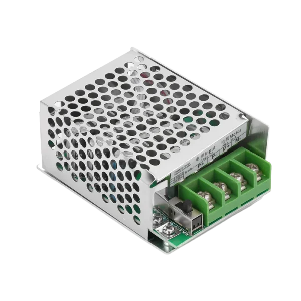 PWM 30A 7-70V DC Motor Speed Controller Module 12V 24V 48V 60V Adjustable Speed Regulator Control Governor Switch
$4.10
PWM 30A 7-70V DC Motor Speed Controller Module 12V 24V 48V 60V Adjustable Speed Regulator Control Governor Switch
$4.10
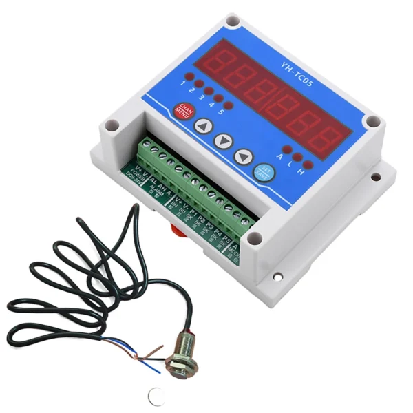 YH-TC05 DC12-24V Tachometer Counter Electronic Digital Display Tachometer Gauge Sensor Non-Contact Motor Speed Meter with Modbus
$2.60 – $15.90Price range: $2.60 through $15.90
YH-TC05 DC12-24V Tachometer Counter Electronic Digital Display Tachometer Gauge Sensor Non-Contact Motor Speed Meter with Modbus
$2.60 – $15.90Price range: $2.60 through $15.90