The copper surface of a printed circuit board is highly reactive. Without protection, it oxidizes rapidly, rendering it unsolderable and increasing contact resistance. The selection of a PCB surface finish is not merely a cost or aesthetic decision; it is a critical metallurgical constraint that dictates the SMT process window, the shelf life of the bare board, the mechanical reliability of the solder joint, and the high-frequency signal integrity.
Choosing an inappropriate finish for a specific application leads to predictable failures: tombstoning on fine-pitch components, brittle solder joints, intermittent high-frequency signal loss, or catastrophic field failures due to dendritic growth. This document analyzes the six primary surface finishes through the lens of manufacturing physics and reliability engineering.
1. HASL (Hot Air Solder Leveling): The Baseline for Through-Hole and Low-Density
HASL involves immersing the PCB in a molten solder bath (typically SAC305 for lead-free or Sn63/Pb37 for legacy applications) and leveling the excess with high-pressure hot air knives.
Metallurgical Reality: HASL leaves a relatively thick coating of solder (typically 100 to 400 microinches). While this provides excellent baseline solderability and a long shelf life, the surface topography is inherently rough.
SMT Constraint: The uneven surface profile (Ra) makes HASL entirely unsuitable for fine-pitch components (≤0.5mm pitch) or BGAs. The varying pad heights cause inconsistent solder paste collapse, leading to bridging or head-in-pillow defects. Furthermore, subjecting a HASL board to multiple reflow cycles accelerates the growth of the Copper-Tin Intermetallic Compound (IMC), which can eventually consume the entire solder layer and cause dewetting.
Application: Low-density boards, through-hole assemblies, and prototype boards where manual soldering is prevalent.
2. ENIG (Electroless Nickel Immersion Gold): The Standard for High-Density Interconnect
ENIG is a dual-layer metallic coating. An electroless nickel layer (typically 120 to 240 microinches) is deposited as a barrier and a robust base for soldering, followed by a thin immersion gold layer (1 to 3 microinches) to protect the nickel during storage. During reflow, the gold dissolves into the solder, and the actual metallurgical bond forms between the solder and the nickel.
Metallurgical Reality: ENIG provides an exceptionally flat surface, making it the mandatory choice for fine-pitch BGAs, QFNs, and edge connectors. However, the process is highly sensitive to bath chemistry.
The "Black Pad" Failure: If the immersion gold process is poorly controlled, the gold layer can cause galvanic corrosion of the underlying nickel, resulting in a brittle, nickel-rich phosphorus layer (the "black pad"). This leads to interfacial fractures under mechanical shock. To mitigate this, manufacturers must strictly control the nickel bath to maintain a medium-phosphorus content (3% to 5%) and ensure the gold layer is thin enough to dissolve completely during reflow.
Application: High-density consumer electronics, servers, telecommunications, and any design utilizing BGA or micro-BGA components.
3. Immersion Tin: The Flat Surface Alternative
Immersion tin deposits a thin layer of pure tin (typically 20 to 40 microinches) onto the copper via a chemical displacement reaction.
Metallurgical Reality: It offers a flat surface comparable to ENIG at a lower cost, and it is lead-free. However, the tin-copper IMC begins forming immediately at the interface.
SMT Constraint: The primary engineering concern is the growth of "tin whiskers"—spontaneous, conductive crystalline structures that can grow millimeters long over time, causing short circuits. Additionally, immersion tin is highly susceptible to organic acid contamination from handling, which rapidly degrades solderability. The shelf life is strictly limited (typically 6 months), and it cannot withstand more than two reflow cycles without significant degradation.
Application: Press-fit connectors, communication backplanes, and cost-sensitive high-density designs where long-term storage is not required.
4. Immersion Silver: The High-Frequency Conductor
Immersion silver deposits a thin layer of pure silver (typically 6 to 12 microinches). Silver has the highest electrical conductivity of all metals, making it highly relevant for high-frequency applications.
Metallurgical Reality: At high frequencies, current flows primarily on the surface of the conductor due to the skin effect. Silver's superior conductivity minimizes insertion loss in RF and microwave circuits.
SMT Constraint: Silver is highly reactive to sulfur and chlorine in the atmosphere, leading to rapid tarnishing (darkening) which destroys solderability. Boards must be packaged in sulfur-free, vacuum-sealed bags with desiccants. Once opened, the boards must be assembled within a strict timeframe (usually 24 to 72 hours).
Application: RF modules, antenna designs, high-speed digital backplanes, and automotive radar systems.
5. OSP (Organic Solderability Preservative): The High-Volume Cost Optimizer
OSP involves applying a microscopically thin (0.2 to 0.5 micrometers) organic film (typically alkylimidazole) onto the bare copper via a conveyorized chemical process. The film prevents oxidation and dissolves instantly when exposed to the thermal shock and flux chemistry of the reflow oven.
Metallurgical Reality: OSP provides a perfectly flat, cost-effective, and environmentally friendly surface.
SMT Constraint: The organic film is fragile. It cannot withstand the mechanical abrasion of ICT (In-Circuit Test) bed-of-nails probes, which will pierce the film and expose the copper to oxidation. Furthermore, OSP boards are highly sensitive to handling (fingerprints degrade the film) and thermal stress. They support a maximum of two to three reflow cycles and have a shelf life of approximately 6 to 9 months.
Application: High-volume consumer electronics, display panels, and cost-optimized motherboards where fine-pitch BGAs are not present.
6. Electroplated Hard Gold: The Wear-Resistant Interface
Electroplated hard gold involves electroplating a thick layer of gold alloyed with cobalt or nickel (typically 30 to 50 microinches or more) over a nickel underplate.
Metallurgical Reality: The alloying elements increase the Knoop hardness, providing extreme wear resistance and low, stable contact resistance over thousands of mating cycles.
SMT Constraint: Hard gold must never be used in areas intended for soldering. If gold is incorporated into a solder joint exceeding 3% by weight, it causes "gold embrittlement," creating a brittle intermetallic compound that fractures under minimal mechanical stress. Hard gold is strictly isolated to edge connectors, keypads, and test points.
Application: Gold fingers, edge card connectors, and sliding electrical contacts.
Validating Surface Finish Compatibility
Selecting a surface finish based on datasheet parameters is insufficient. The interaction between the specific solder paste alloy, the reflow profile, and the surface finish must be physically validated. For instance, verifying the absence of black pad in ENIG or confirming the tin whisker mitigation strategy in Immersion Tin requires physical cross-sectioning and aging tests.
Iterating through multiple bare board builds to test different surface finishes under actual thermal stress can deplete prototyping budgets. To facilitate rapid physical validation of surface finish reliability, we maintain a strategic initiative: $2 for 5 pieces for any custom PCB under 50mm x 50mm.
This allows engineering teams to manufacture dedicated test coupons, subject them to multiple thermal cycling profiles, and perform metallographic cross-sections to evaluate IMC growth and solder joint integrity without the financial friction that typically delays critical material validation.
Scaling Surface Finish Consistency to Mass Production
Achieving a defect-free surface finish on a 5-piece prototype is fundamentally different from maintaining that quality across a 50,000-unit production run. In mass production, the degradation of chemical bath concentrations, the buildup of metallic impurities (such as palladium or copper in the ENIG line), and the fluctuation of OSP film thickness directly translate into SMT yield losses.
Transitioning to high-volume manufacturing requires a partner with rigorous chemical process control and automated dosing systems. By utilizing our turnkey PCB prototype and assembly manufacturing services, the exact surface finish parameters validated during your prototype phase are locked into the mass-production control plan. Our SMT engineers will adjust the stencil aperture and reflow profile specifically for the chosen finish, ensuring optimal wetting and minimizing defects like tombstoning or voiding.
When your design is validated and you are ready to secure long-term material allocation and optimize panelization for your specific surface finish requirements, initiating an OEM/ODM bulk manufacturing inquiry allows our process engineering team to align your supply chain with our strict statistical process control (SPC) protocols.
FAQ
Q: How do we prevent "Black Pad" (brittle fracture) in ENIG finishes?
A: Black pad is caused by the excessive corrosion of the nickel layer during the gold displacement reaction. We prevent this by strictly maintaining the nickel bath at a medium-phosphorus level (3-5%), ensuring the immersion gold layer is kept as thin as possible (1-2 microinches) so it fully dissolves during reflow, and implementing strict bath life management to prevent palladium contamination.
Q: Why can't I use Electroplated Hard Gold for my solder pads?
A: Hard gold is alloyed with cobalt or nickel to increase hardness. If this gold enters the molten solder joint and exceeds 3% by weight, it forms a highly brittle gold-tin intermetallic compound. This "gold embrittlement" causes the solder joint to crack under minimal mechanical or thermal stress. Hard gold must be strictly limited to contact surfaces.
Q: What is the maximum number of reflow cycles an OSP finish can withstand?
A: OSP is generally limited to two, maximum three, reflow cycles. Beyond this, the organic film degrades, and the underlying copper oxidizes, leading to severe non-wetting defects. For designs requiring multiple reflow cycles (e.g., double-sided SMT or press-fit insertion after reflow), ENIG or Immersion Silver must be specified.
Q: How do you mitigate the risk of Tin Whiskers in Immersion Tin finishes?
A: Tin whisker growth is driven by compressive stress in the tin layer. We mitigate this by strictly controlling the immersion tin bath chemistry, applying a post-deposition baking process (annealing) to relieve internal stress, and ensuring the final tin layer thickness is tightly controlled. For mission-critical applications, we recommend ENIG instead.
The selection of a PCB surface finish is a complex trade-off between solderability, shelf life, planarity, high-frequency performance, and cost. It requires a clear understanding of the metallurgical interactions at the solder joint interface and the physical limitations of the SMT process.

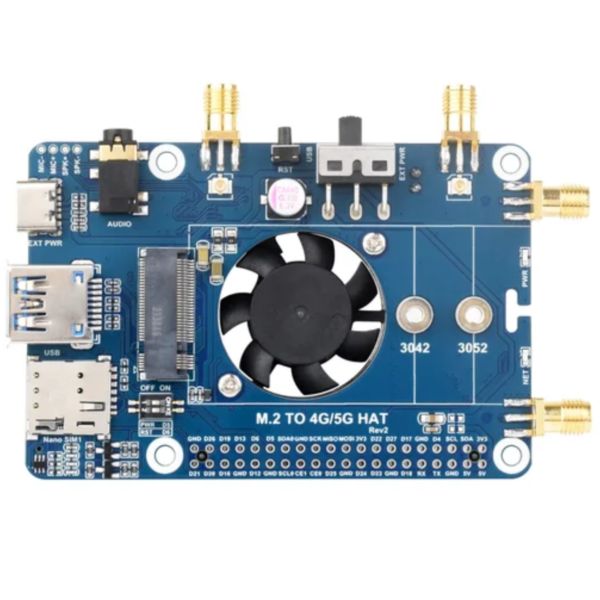 SIM7600G-H M.2 4G HAT, 4G/3G/2G Communication And GNSS Positioning for Raspberry Pi LTE
$95.90
SIM7600G-H M.2 4G HAT, 4G/3G/2G Communication And GNSS Positioning for Raspberry Pi LTE
$95.90
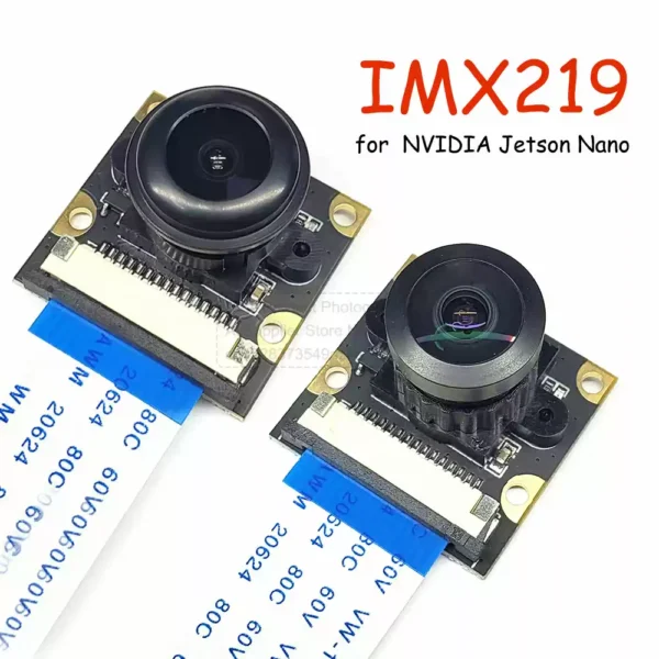 IMX219 Camera Module – 8MP HD, Adjustable Focus, Available in 77°/120°/130°/200°/160°/222° FOV Options
$6.90 – $18.90Price range: $6.90 through $18.90
IMX219 Camera Module – 8MP HD, Adjustable Focus, Available in 77°/120°/130°/200°/160°/222° FOV Options
$6.90 – $18.90Price range: $6.90 through $18.90
 LOOI Smart Desktop Robot | AI Desktop Companion,ChatGPT Voice Interaction,Memory,Gesture& Face Recognition,Emotional Support
$219.80
LOOI Smart Desktop Robot | AI Desktop Companion,ChatGPT Voice Interaction,Memory,Gesture& Face Recognition,Emotional Support
$219.80
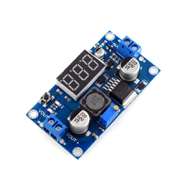 LM2596 DC DC Step Down Converter Voltage Regulator LED Display Voltmeter 4.0~40 to 1.3-37V Buck Adapter Adjustable Power Supply
$3.50
LM2596 DC DC Step Down Converter Voltage Regulator LED Display Voltmeter 4.0~40 to 1.3-37V Buck Adapter Adjustable Power Supply
$3.50
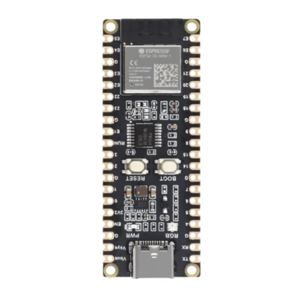 ESP32-C6 Microcontroller for ESP-IDF, Arduino, 160MHz RISC-V 32-bit Single-core Processor, ESP32-C6-MINI-1 Module
$8.50 – $9.50Price range: $8.50 through $9.50
ESP32-C6 Microcontroller for ESP-IDF, Arduino, 160MHz RISC-V 32-bit Single-core Processor, ESP32-C6-MINI-1 Module
$8.50 – $9.50Price range: $8.50 through $9.50