A two-terminal component shouldn't be this hard to get right. Yet, diode selection remains one of the most frequent sources of latent PCBA failures we encounter during Design for Manufacturability (DFM) reviews.
The pattern is painfully predictable: an engineer grabs a 1N4007 for a 150kHz flyback output, specifies a 40V Schottky on a 12V rail without calculating the reflected voltage spike, or places a high-capacitance TVS on a USB 3.0 data line and wonders why the signal eye diagram collapses. The board passes initial functional testing on the bench, ships to the customer, and then the field returns start piling up—thermal runaway, surge damage, intermittent communication failures.
This guide cuts through the datasheet noise. We will walk through the parameters that actually matter in real operating conditions, break down the selection logic for each diode family, and highlight the five most expensive mistakes we see in incoming BOM reviews.
The Parameters That Bite You in Production
Datasheets list dozens of specifications, but in our experience reviewing thousands of PCBA designs, these are the parameters that cause the most field failures when misunderstood.
VRRM (Maximum Repetitive Reverse Voltage): This is your hard ceiling. The periodic reverse voltage in your circuit must never exceed this value. The datasheet also lists VRSM (non-repetitive peak), which is typically 1.2x to 1.5x higher—but that margin exists for single-event surges, not continuous operation. Design to VRRM with a 1.2x to 1.5x safety factor that accounts for grid transients and parasitic ringing.
VF (Forward Voltage Drop): The "silicon is 0.7V, Schottky is 0.3V" rule of thumb is dangerously misleading. VF rises with current and falls with temperature (approximately -2mV/°C). If you calculate conduction losses using the room-temperature, low-current datasheet value, your actual power dissipation at full load in a 60°C enclosure can be off by a factor of two or more.
IR (Reverse Leakage Current): This is the silent killer in high-temperature environments. Standard silicon diodes roughly double their leakage every 10°C. Schottky diodes are far worse—their leakage can increase by two to three orders of magnitude (100x to 1000x) from 25°C to 100°C. At elevated temperatures, the leakage-induced power dissipation (VR × IR) can exceed the conduction loss (VF × IF), triggering a positive thermal feedback loop that destroys the component.
trr and Qrr (Reverse Recovery): For switching power supplies above 100kHz, trr alone is insufficient. The actual switching loss is better estimated by Prr ≈ Qrr × Vreverse × fsw. A diode with a short trr but large Qrr can dissipate more heat than one with a slightly longer trr but lower stored charge. This distinction is critical when evaluating fast recovery diodes for PFC stages and motor drive inverters.
Selecting by Application: What Actually Goes on Your Board
Rather than memorizing material science classifications, focus on the functional role each diode plays in your circuit and the failure modes specific to that role.
Power Rectification (AC-DC and DC-DC Output)
For 50/60Hz mains rectification, the 1N4007 (1A/1000V) remains the workhorse. But the moment your switching frequency exceeds 100kHz, its 2–4µs reverse recovery time becomes a thermal disaster. For low-voltage, high-current outputs (5V/3A, 12V/2A), replace it with a Schottky like the SS34 (40V/3A, VF ≈ 0.4V) or, for even higher efficiency, move to synchronous rectification with a low-RDS(on) MOSFET.
For high-voltage, high-frequency applications (PFC stages, industrial inverters), fast recovery diodes like the MUR460 (4A/600V, trr ≈ 50ns) are mandatory. If your product must pass stringent EMC standards (medical, automotive, telecom), specifically request soft-recovery variants to minimize high-frequency ringing caused by hard snap-off characteristics.
Schottky and the SiC Revolution
Silicon Schottky diodes dominate low-voltage DC-DC converters due to their near-zero reverse recovery and low VF. However, their reverse voltage ceiling (typically <200V) and extreme temperature-dependent leakage limit their use in high-voltage designs.
The emergence of Silicon Carbide (SiC) Schottky diodes has fundamentally changed this trade-off. Devices like the C4D40120D (1200V/27A) offer near-zero reverse recovery at voltages where silicon Schottky cannot operate, with switching characteristics that remain stable across temperature. They are rapidly replacing silicon fast recovery diodes in EV on-board chargers, server power supplies, and solar inverters.
TVS Diodes for Surge and ESD Protection
TVS selection is where we see the highest density of BOM errors. Three rules are non-negotiable:
- VCL (Clamping Voltage) must be below the absolute maximum rating of the downstream IC. A TVS with the correct VRWM and VBR is useless if its clamping voltage during a surge exceeds what the protected chip can survive.
- Junction capacitance (Cj) must match the signal speed. On USB 3.0, HDMI, or Gigabit Ethernet lines, Cj must be below 1pF to preserve signal integrity. On low-speed power inputs, several hundred pF is perfectly acceptable—do not waste budget on ultra-low-capacitance TVS arrays where they are not needed.
- Never use a TVS as a continuous voltage regulator. TVS devices are rated for kilowatt-level pulse power but only a few watts of continuous dissipation. Sustained operation in breakdown will destroy them in seconds.
Five Selection Mistakes That Survive Prototype Testing but Fail in the Field
Mistake 1: Using a 1N4007 in a switching power supply output. The static voltage and current ratings look adequate, but at 100kHz+, the 2–4µs trr causes massive cross-conduction losses. The diode overheats and the efficiency collapses.
Mistake 2: Underestimating Schottky reverse voltage stress. A 40V Schottky on a 12V flyback output seems safe until you calculate the reflected voltage spike: Vrec_peak = Vo + (Vin_max / Nps) × Nsec. The actual reverse stress frequently reaches 30–40V, leaving almost no margin. Combined with the 100x leakage increase at 100°C, the design is operating on the edge of thermal runaway.
Mistake 3: Zener diodes without a current-limiting resistor. Connecting a Zener diode directly across a voltage source will destroy it instantly. Always include a series resistor (R = (Vin - VZ) / IZ) to limit the current to the specified test current (IZ).
Mistake 4: Placing high-capacitance TVS on high-speed data lines. A standard TVS with 50pF junction capacitance on a USB 3.0 differential pair will destroy the signal eye diagram. Use dedicated low-capacitance ESD protection arrays (<1pF) for any interface above 1Gbps.
Mistake 5: Evaluating efficiency using only VF × IF. Total diode loss equals conduction loss (VF × IF) plus blocking loss (VR × IR). At high temperatures and high reverse voltages, the IR component can dominate. Always evaluate both terms across the full operating temperature range.
Bridging Component Selection to PCBA Assembly Reality
Selecting the right diode on paper is only half the battle. The physical realities of SMT assembly introduce additional constraints that must be addressed before your board hits the production line.
Package and Thermal Considerations: A DO-41 through-hole diode rated at 1A may not survive 0.5A inside a sealed enclosure without a heatsink. When transitioning to surface-mount packages for automated assembly, verify that the chosen footprint (SMA, SMB, SMC) provides adequate copper pour area for thermal dissipation. An SMA package can typically handle 1–2A with proper thermal vias; SMC is required for 3A and above.
SMT Process Compatibility: Small packages like SOD-123 are prone to tombstoning during reflow if the pad geometry is asymmetric or the thermal relief is unbalanced. During our DFM review, we routinely flag these risks and recommend pad modifications before the first prototype spin.
Moisture Sensitivity and Automotive Qualification: If your diode carries an MSL (Moisture Sensitivity Level) rating of 2 or higher, it must be assembled within the specified floor life after opening the moisture barrier bag, or pre-baked before reflow. For automotive applications, AEC-Q101 qualification is a hard requirement—no exceptions.
Validating Your Diode Selection on Real Hardware
Simulation models and datasheet calculations provide a starting point, but the only way to confirm your diode selection under real thermal and electrical stress is to build the physical board and measure it.
Thermal runaway in Schottky diodes, reverse recovery losses in fast recovery devices, and TVS clamping behavior under actual surge conditions all require physical validation. Iterating through multiple prototype spins to test different diode candidates and thermal layouts can quickly consume your R&D budget.
To remove this financial barrier, we maintain a dedicated prototyping initiative: $2 for 5 pieces for any custom PCB under 50mm x 50mm. Use it to spin test coupons that validate your diode thermal performance, verify your TVS protection network under real surge conditions, and compare different package footprints on your actual stack-up—without the cost pressure that forces engineers to skip critical validation steps.
From Validated Design to Reliable Mass Production
Once your diode selection is proven and your thermal design is locked, the challenge shifts to ensuring that every board coming off the line performs identically. A component substitution by an unauthorized distributor, a reflow profile that exceeds the diode's maximum junction temperature, or a misplaced TVS due to a polarity error in the pick-and-place program can undo months of careful design work.
Our turnkey PCB prototype and assembly manufacturing service addresses this by maintaining strict BOM control, sourcing all diodes and semiconductors from authorized tier-1 distributors, and locking your validated reflow profiles into the production control plan. The same engineering team that reviewed your diode selection during prototyping oversees the assembly line.
When your project transitions to high-volume production, initiating an OEM/ODM bulk manufacturing inquiry allows us to secure long-term component allocation, negotiate volume pricing on your specific diode requirements, and implement automated optical inspection (AOI) programs tuned to catch polarity and placement errors on every board.
FAQ
Q: How do I choose between a Schottky diode and a fast recovery diode for my power supply?
A: For output voltages below 48V and switching frequencies above 100kHz, Schottky diodes offer superior efficiency due to their low VF and near-zero reverse recovery. For high-voltage applications (above 200V) such as PFC stages or industrial inverters, fast recovery diodes are required due to their higher voltage ratings. For the best of both worlds at high voltage, consider SiC Schottky diodes.
Q: Why is my Schottky diode overheating even though the current is well below its rated value?
A: Schottky reverse leakage current (IR) increases exponentially with temperature—often by 100x to 1000x from 25°C to 100°C. At high ambient temperatures and high reverse voltages, the blocking loss (VR × IR) can exceed the conduction loss (VF × IF), triggering thermal runaway. Always evaluate total power dissipation across the full operating temperature range.
Q: What junction capacitance should I specify for TVS diodes on high-speed interfaces?
A: For USB 3.0, HDMI, Gigabit Ethernet, and any differential interface above 1Gbps, the TVS junction capacitance must be below 1pF per line to prevent signal integrity degradation. For low-speed power inputs and GPIO lines, several hundred pF is acceptable and significantly less expensive.
Q: Can your assembly facility handle AEC-Q101 qualified diodes for automotive PCBA?
A: Yes. We source all automotive-grade components exclusively from authorized distributors with full lot traceability and AEC-Q101 certification. Our assembly processes comply with IPC-A-610 Class 3 standards required for automotive electronics.
A diode is a physical device governed by thermodynamics, semiconductor physics, and parasitic effects—not an ideal symbol in a SPICE schematic. Every selection decision involves trade-offs between forward loss, reverse leakage, switching speed, thermal stability, and package constraints. The engineers who internalize these trade-offs are the ones whose boards survive the transition from prototype to mass production without costly field returns.
If your next design involves high-frequency power conversion, surge protection, or automotive-grade reliability requirements, send your schematic and BOM to our engineering team. We will review your diode selections against real-world operating conditions and SMT assembly constraints before your first prototype spin.

 Small Blackboard Eight-way Transponder Kit SYB52 Multi-way Robotic Test Practical Training elding Electronic Fabrication Kit
$4.90
Small Blackboard Eight-way Transponder Kit SYB52 Multi-way Robotic Test Practical Training elding Electronic Fabrication Kit
$4.90
 Photosensitive Sensor Module 3Pin 3.3V-5V Photoresistor Light Detection Resistance Module Photo Resistor for Arduino
$1.90
Photosensitive Sensor Module 3Pin 3.3V-5V Photoresistor Light Detection Resistance Module Photo Resistor for Arduino
$1.90
 Mini USB Fan Governor Wind Speed Controller Air Volume Regulator Cooling Mute Multi Function Fan Speed Switch Module DC 5V
$6.50
Mini USB Fan Governor Wind Speed Controller Air Volume Regulator Cooling Mute Multi Function Fan Speed Switch Module DC 5V
$6.50
 DC-DC Buck Boost Converter Module 5.5-30V to 0.5-30V 4A 35W Adjustable Step Up Down Voltage Regulator LCD Digital Voltmeter
$3.90
DC-DC Buck Boost Converter Module 5.5-30V to 0.5-30V 4A 35W Adjustable Step Up Down Voltage Regulator LCD Digital Voltmeter
$3.90
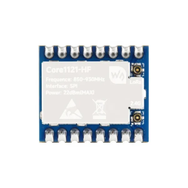 Core1121 LF/HF Dual-Band LoRa Module, Based on Low-Power LR1121 Transceiver, Suitable For Sub-GHz And 2.4GHz Frequency Bands