In modern electronics manufacturing, Surface Mount Technology (SMT) is often misunderstood as merely a mechanical process of placing components onto a board. In reality, high-reliability SMT is a rigorous science of material physics, environmental control, and statistical process management.
For hardware engineers and quality managers, a single deviation in solder paste viscosity, a minor fluctuation in the reflow profile, or an ungrounded operator can trigger catastrophic field failures. Latent defects do not show up during initial functional testing; they manifest months later in the field as intermittent connections or sudden component degradation.
This guide bypasses generic textbook definitions. We will dissect the critical shop-floor control parameters for SMT assembly and Electrostatic Discharge (ESD) protection, providing the exact engineering standards required to achieve zero-defect PCBA manufacturing.
Pillar 1: Environmental and Material Integrity
The foundation of a reliable solder joint is established long before the board enters the pick-and-place machine. It begins with strict environmental and material lifecycle management.
Ambient Control and MSD Baking
The SMT production environment must be strictly maintained at ≤25°C and ≤60% Relative Humidity (RH). Deviations cause moisture absorption in both the PCB substrate and Moisture-Sensitive Devices (MSDs), leading to "popcorn" cracking during reflow.
- Standard PCBs/Components: Must be baked at 100°C–120°C for 4 hours if exposed beyond their floor life.
- Vacuum-Packaged BGA: Requires baking at 100°C–125°C for 4 hours once the seal is broken.
- Loose or Anti-Static Bagged BGA: Requires an extended bake of 24 hours at 100°C–125°C to drive out deeply absorbed moisture.
- Control Point: Oven temperatures must be logged by dedicated SMT personnel every 2 hours. If baked components exceed their allowable floor time (e.g., 72 hours for PCBs, 6 hours for BGA), the baking cycle must be restarted.
Solder Paste Lifecycle Management
Solder paste is a living chemical mixture. Mismanagement here is the primary cause of bridging, tombstoning, and voiding.
- Storage & Thawing: Must be stored at 4°C–10°C. Upon removal, it requires a minimum of 4 hours to reach room temperature before opening to prevent condensation.
- Mixing & Viscosity: Mechanical stirring for 3–5 minutes is mandatory. The target viscosity must be maintained between 180 and 260 kcps (kilopoise).
- Printing Parameters: Squeegee pressure is typically set around 5 kg, with a speed of 20–50 mm/s. The deposited paste thickness should be 1.0 to 1.5 times the stencil thickness (e.g., a 0.12mm stencil yields 0.12–0.18mm paste).
- Rework Limits: Solder paste returned to the jar can be mixed with fresh paste, but this rework cycle must not exceed two times.
- Maintenance: Stencil under-cleaning must occur every 30 minutes for semi-auto printers, or every 100 boards for fully automated lines, to prevent aperture clogging.
Pillar 2: Precision in Assembly and Reflow Profiling
Once materials are prepared, the focus shifts to mechanical precision and thermal dynamics.
Feeder Validation and First Article Inspection (FAI)
Material mix-ups are a leading cause of mass rework. SMT IPQC (In-Process Quality Control) must verify every feeder against the machine’s axis load list, checking part numbers, specifications, and tolerance values. For loose components, LCR meter verification is mandatory before loading. Following setup, a strict three-tier FAI process is enforced: Technician setup → Line Leader verification → IPQC final sign-off. The approved first article is retained as the golden sample for the entire production run.
The Reflow Soldering Profile
The reflow oven is where the metallurgical bond is formed. A standard lead-free profile consists of four critical zones, which must be validated with a 4-to-6 point thermocouple profile:
- Preheat: Gradual ramp to activate the flux without thermal shock.
- Soak (Thermal Equalization): 140°C–180°C for 40–60 seconds. This ensures the entire board, including heavy copper planes, reaches a uniform temperature.
- Reflow (Peak): 210°C–240°C for 60–90 seconds (never dropping below 45 seconds above liquidus). This melts the solder and forms the intermetallic compound (IMC).
- Cooling: Controlled natural cooling. Rapid quenching is strictly prohibited, as it induces thermal shock and micro-cracking in ceramic capacitors.
Pillar 3: Post-Soldering Cleaning and Residue Control
For applications requiring high reliability, flux residues must be removed to prevent electrochemical migration (dendrite growth) and corrosion.
Deionized Water Washing Parameters
Aqueous cleaning systems must operate within strict chemical and mechanical boundaries:
- Water Quality: Temperature at 30°C–35°C, pH strictly between 6.5 and 8.5, and Total Dissolved Solids (TDS) must remain <8 PPM.
- Spray Pressure:
- Zone 1: Top 1.5–3.0 kg/cm², Bottom 4.6–5.5 kg/cm².
- Zone 2: Top 4.6–5.5 kg/cm², Bottom 3.0–4.5 kg/cm².
- Zone 3: Top pressure must always exceed bottom pressure by at least 0.05 kg/cm² to prevent water trapping under components.
- Drying: Multi-zone drying ovens (e.g., Zone 1 at 135°C ±5°C, Zone 2 at 140°C ±5°C) with precisely calibrated conveyor speeds ensure zero moisture retention.
Pillar 4: The Invisible Killer – ESD Protection Protocol
In microelectronics, Electrostatic Discharge (ESD) is a silent destroyer. A human walking across a carpet can generate 3,000V of static electricity. While harmless to humans, a discharge of merely 250V can permanently degrade or destroy sensitive semiconductor junctions.
The Danger of Latent ESD Failure
ESD damage is not always catastrophic (immediate failure). More dangerously, it causes latent failures, where the component’s internal oxide layer or P-N junction is partially degraded. The board passes initial testing but fails prematurely in the field, leading to costly warranty claims and brand damage.
The Three Vectors of ESD Damage
- Human Body Model (HBM): An operator touches a sensitive component, discharging built-up body static directly into the device.
- Device Charging Model (CDM): The component itself becomes charged through friction with plastic trays or tapes, then discharges rapidly upon contact with a grounded surface.
- Field Induction: A charged object near the PCB induces a voltage potential in the traces, causing internal arcing.
Mandatory Shop-Floor ESD Controls
- Personnel Grounding: Operators handling ESD-sensitive devices must wear grounded wrist straps, tested and logged daily. Resistance to ground must be between 0.75MΩ and 1.5MΩ.
- Workstation Grounding: ESD mats and equipment chassis must be bonded to a common ground point with resistance <1Ω.
- Ionization: In areas where insulating materials (like standard plastic component reels) cannot be grounded, ionizing air blowers must be used to neutralize surface charges via corona discharge.
- Shielding: All sensitive components must be transported and stored in metallized static-shielding bags, never in standard clear plastic.
Validating Process Parameters: The Cost of Physical Iteration
Documenting these parameters in a Standard Operating Procedure (SOP) is only the first step. The true challenge is validating that your specific board design can withstand these processes without warpage, solder bridging, or ESD damage.
Iterating through multiple prototype builds to fine-tune your stencil design, reflow profile, and ESD handling protocols can rapidly deplete an R&D budget.
This is not a marketing gimmick; it is a strategic engineering tool. It allows your team to:
- Print physical test coupons to verify solder paste deposition and reflow behavior on your specific stack-up.
- Validate ESD shielding and grounding point placements on real hardware.
- Iterate on component footprints and thermal relief designs without financial penalty.
Transitioning to Volume: Securing Consistent Quality at Scale
Once your prototype has proven that the design can survive rigorous SMT and ESD controls, the focus shifts to mass production consistency. A process that works for 10 boards must be statistically locked for 10,000 boards.
Scaling requires a partner who treats process control not as a checklist, but as a core business philosophy. By utilizing our turnkey PCB prototype and assembly manufacturing services, you ensure that the exact reflow profiles, stencil apertures, and FAI protocols validated during prototyping are seamlessly transferred to the mass-production control plan.
When you are ready to secure long-term component allocation, implement automated optical inspection (AOI) tuning, and establish a fully traceable supply chain, initiating an OEM/ODM bulk manufacturing inquiry allows our engineering team to align your BOM and layout with high-volume, zero-defect manufacturing methodologies.
FAQ
Q: What is the absolute maximum number of times solder paste can be reworked?
A: Solder paste should never be reworked more than two times. Each exposure to ambient air and mechanical stirring degrades the flux chemistry and alters the viscosity, leading to poor wetting and increased voiding during reflow.
Q: Why is latent ESD failure more dangerous than catastrophic failure?
A: Catastrophic failure is caught during initial Functional Circuit Testing (FCT). Latent failure means the component is partially degraded but still functions initially. It will fail unpredictably in the field, leading to expensive warranty claims, safety hazards, and irreversible brand damage.
Q: How often should the reflow oven temperature profile be audited?
A: Best practice dictates a full thermocouple profile audit at the start of every shift, after any machine maintenance, or whenever a new board design with significantly different thermal mass is introduced to the line.
Q: What are the critical water quality metrics for post-soldering cleaning?
A: To prevent ionic contamination and corrosion, the deionized water must maintain a pH between 6.5 and 8.5, and the Total Dissolved Solids (TDS) must be strictly kept below 8 PPM.
Translating documented SOPs into consistent shop-floor discipline is the defining characteristic of a world-class electronics manufacturer. It requires relentless attention to humidity levels, solder paste chemistry, thermal profiling, and electrostatic discharge protocols.

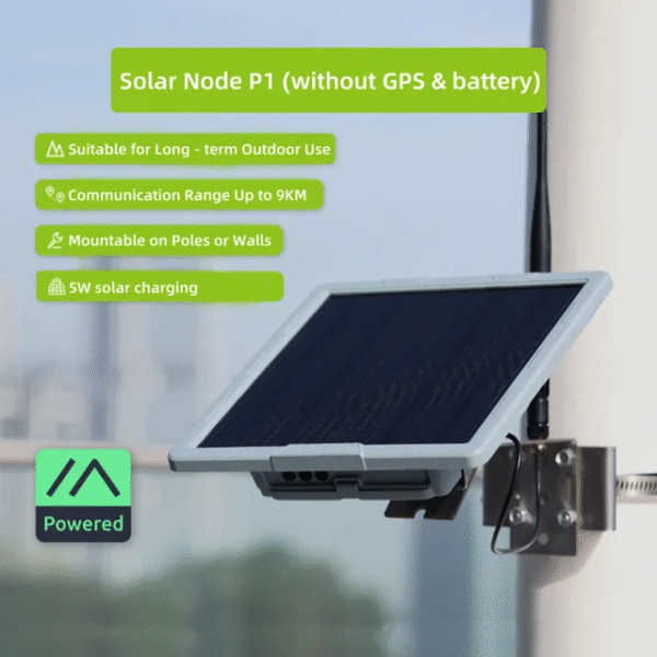 SenseCAP Meshtastic Solar Node, 5W Solar Power Mesh LoRa Node, Integrates XIAO nRF52840 Plus,-SX1262 LoRa Module,Grove, L76K GPS
$92.90 – $120.90Price range: $92.90 through $120.90
SenseCAP Meshtastic Solar Node, 5W Solar Power Mesh LoRa Node, Integrates XIAO nRF52840 Plus,-SX1262 LoRa Module,Grove, L76K GPS
$92.90 – $120.90Price range: $92.90 through $120.90
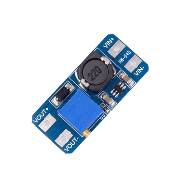 5PCS MT3608 Boost Module DC-DC Step Up Converter Booster Power Supply Module Board Max 2A 2V-24V To 5/9/12/28V for Arduino
$3.90
5PCS MT3608 Boost Module DC-DC Step Up Converter Booster Power Supply Module Board Max 2A 2V-24V To 5/9/12/28V for Arduino
$3.90
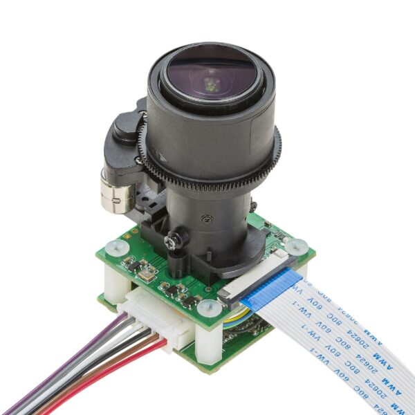 Arducam 5MP 1080p Pan Tilt Zoom PTZ Camera for Raspberry Pi 4/3B+/3
$139.60
Arducam 5MP 1080p Pan Tilt Zoom PTZ Camera for Raspberry Pi 4/3B+/3
$139.60
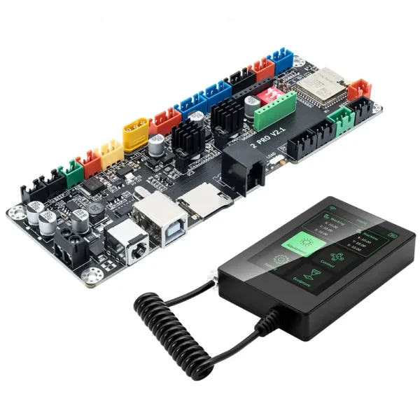 For CNC Engraving Machine Makerbase MKS LS ESP32 PRO GRBL Controller Module Support WIFI Bluetooth Touch Screen Upgrade DLC32
$18.90 – $42.90Price range: $18.90 through $42.90
For CNC Engraving Machine Makerbase MKS LS ESP32 PRO GRBL Controller Module Support WIFI Bluetooth Touch Screen Upgrade DLC32
$18.90 – $42.90Price range: $18.90 through $42.90
 T-Display-S3 ESP32-S3 1.9 Inch ST7789 LCD Display Development Board WIFI Bluetooth5.0 Wireless Module 170X320 Resolution
$18.90
T-Display-S3 ESP32-S3 1.9 Inch ST7789 LCD Display Development Board WIFI Bluetooth5.0 Wireless Module 170X320 Resolution
$18.90