When hardware teams tackle high-speed digital designs—whether it is DDR4/5, Gigabit Ethernet, USB 3.x, MIPI, or multi-gigabit SerDes channels—the first prototype spin almost always fails. The symptoms are universally frustrating: closed eye diagrams, soaring bit error rates (BER), failed EMC compliance, or intermittent system reboots.
Engineers often spend weeks probing clocks and power rails with oscilloscopes, only to realize the root cause lies in a fundamental cognitive gap: applying low-frequency "point-to-point" routing logic to microwave-level electromagnetic waves.
Once signal rise times shrink into the sub-nanosecond range, Kirchhoff's circuit laws no longer apply. Traces are no longer simple wires; they are complex transmission lines guiding electromagnetic energy. This guide bridges the gap between Signal Integrity (SI) theory and physical PCB manufacturing, detailing the critical Design for Manufacturability (DFM) rules required to ensure your high-speed boards succeed on the first pass.
The True Definition of "High-Speed": It's All About Rise Time
A common trap for junior engineers is defining "high-speed" solely by the data rate (e.g., "This is a 1 Gbps signal"). This is a critical mistake. The parameter that dictates whether a trace must be treated as a controlled-impedance transmission line is the signal rise time (trtr), not the clock frequency.
Even a 10 MHz clock signal can contain high-frequency harmonics well into the hundreds of megahertz if its edge transition is steep (e.g., tr=1 nstr=1 ns).
The Bandwidth Rule
From a Fourier analysis perspective, a digital pulse is composed of a fundamental frequency and a series of high-order harmonics. To preserve the sharp edges of the signal at the receiver, the PCB trace must pass these harmonics without severe attenuation. The effective bandwidth (BWBW) required to preserve the rise time is calculated using the industry-standard formula:
BW≈0.35/trBW≈0.35/tr
For a signal with a 1 ns rise time, the trace must support a bandwidth of 350 MHz. For a 100 ps rise time, the required bandwidth skyrockets to 3.5 GHz. At these frequencies, the parasitic capacitance, skin effect, and dielectric losses of the FR-4 substrate will aggressively attenuate high-order harmonics, causing the signal edges to round off and the timing margins to collapse.
The Transmission Line Threshold
When does a simple trace become a transmission line? According to signal integrity authorities like Howard Johnson and Eric Bogatin, if the trace propagation delay (TDTD) exceeds 1/6th to 20% of the signal rise time (TD>tr/6TD>tr/6), distributed parameters take over. Reflections, ringing, and crosstalk will severely degrade the signal unless strict impedance control and termination strategies are applied.
The 3 Fatal Flaws in High-Speed PCB Routing
If you treat high-speed traces as simple connections, three physical phenomena will destroy your signal integrity:
- Impedance Discontinuity: When a signal encounters a change in trace width, a layer transition via, or a variation in dielectric thickness, the characteristic impedance shifts. This causes a portion of the signal energy to reflect back to the source, creating ringing and reducing the vertical opening of the eye diagram.
- Return Path Disruption: High-frequency return currents naturally flow on the reference plane directly beneath the signal trace to minimize loop inductance. If the signal crosses a split ground plane or a cutout, the return current is forced to detour. This massive increase in loop area acts as an antenna, causing severe EMI radiation and crosstalk.
- Crosstalk: Electromagnetic coupling between adjacent parallel traces. To suppress crosstalk, high-speed signals must be tightly coupled to their reference planes, keeping the electromagnetic fields confined between the trace and the ground plane.
The Manufacturing Reality: Where Simulations Meet the Factory Floor
A flawless SI simulation is useless if the PCB fabricator cannot physically manufacture the board to your tolerances. Here is how advanced manufacturing capabilities directly impact high-speed performance.
1. Precision Impedance Control & Material Selection
Achieving a target impedance (e.g., 50Ω single-ended, 100Ω differential) requires more than just calculating trace widths. It demands strict process control on the factory floor.
- LDI (Laser Direct Imaging): Top-tier manufacturers use LDI instead of traditional film photoplotters to achieve ultra-precise trace widths and spacing, which is the foundation of accurate differential impedance.
- Vacuum Lamination: High-end vacuum lamination presses ensure precise control over the dielectric thickness (prepreg flow), preventing impedance variations across the panel.
- Material Consistency: Standard FR-4 is insufficient for multi-gigabit signals due to high dielectric loss (DfDf). For 10Gbps+ designs, manufacturers must utilize low-loss materials like Megtron, Isola, or Rogers RO4350B, ensuring batch-to-batch consistency in Dielectric Constant (DkDk).
2. Via-in-Pad (VIPPO) for BGA Fanout
When routing out of fine-pitch BGAs (e.g., 0.8mm or 0.65mm pitch), traditional "dog-bone" fanout consumes too much surface routing space. Via-in-Pad Plated Over (VIPPO) places the via directly inside the SMT pad.
- The Manufacturing Reality: To prevent solder paste from wicking down the via during reflow (causing cold joints), the via must be resin-filled, cured, planarized, and copper-capped. This creates a perfectly flat surface for SMT assembly while minimizing the parasitic inductance of the via stub, preserving signal integrity for DDR and SerDes channels.
3. Back-Drilling to Eliminate Via Stubs
For signals exceeding 5 Gbps (e.g., PCIe Gen3/4, 10G Ethernet), the unused portion of a through-hole via (the "stub") acts as an open-circuited transmission line stub. This stub creates a severe resonant notch in the insertion loss (S21S21) at specific frequencies.
The resonant frequency of the stub is approximated by: fres≈c/(4×Lstub×ϵr)fres≈c/(4×Lstub×ϵr)
If this notch falls within the signal's bandwidth, the eye diagram will close completely. To fix this, manufacturers use Back-Drilling—a secondary drilling process using a slightly larger drill bit to remove the unused copper stub from the bottom of the board. For 10Gbps signals, the residual stub length must be strictly controlled to less than 8 mils (0.2mm) to prevent signal degradation.
The Startup Advantage: Rapid High-Speed Prototyping Without Financial Risk
Designing high-speed boards requires rigorous physical validation. You cannot rely solely on 2D simulations; you must test the actual impedance, crosstalk, and via performance on physical hardware. Iterating through multiple prototype spins to perfect your stack-up and routing can rapidly drain a startup's R&D budget.
This is not a gimmick; it is a strategic engineering tool. It allows you to:
- Validate Impedance Coupons: Test your calculated stack-up and trace widths on real FR-4 or high-frequency materials.
- Iterate Fearlessly: Test different via topologies, ground stitching patterns, or BGA fanout strategies without financial penalty.
- Accelerate R&D: Order multiple layout variants simultaneously to compare real-world TDR (Time Domain Reflectometry) results.
Scaling Your Design: From DFM to Turnkey Mass Production
Once your high-speed layout is validated and your prototype passes TDR and eye-diagram testing, the focus shifts to scalable assembly. A flawless bare board can still be ruined by poor solder paste volume on BGA pads, misaligned stencils, or counterfeit components during the PCBA phase.
Transitioning from a validated prototype to mass production requires a partner who understands the intricate relationship between bare board fabrication and SMT assembly. By utilizing our turnkey PCB prototype and assembly manufacturing services, you ensure that the CAM engineers reviewing your Gerber files are the same experts managing your SMT lines. They will optimize your stencil apertures specifically for your fine-pitch BGA and via-in-pad design, guaranteeing perfect solder paste deposition and eliminating cold joints.
If you are preparing to scale your product line and need to optimize panelization, secure allocation for high-speed ICs, and drive down per-unit costs, initiating an OEM/ODM bulk manufacturing inquiry early in your design cycle allows our engineering team to align your BOM and layout with the most cost-effective mass-production methodologies.
FAQ
Q: How do I determine if my PCB trace needs to be treated as a transmission line?
A: Do not rely on the clock frequency. Calculate the signal's rise time (trtr). If the trace's propagation delay (TDTD) is greater than 1/6th of the rise time (TD>tr/6TD>tr/6), it must be designed as a controlled-impedance transmission line with strict return path management.
Q: Why is my 50Ω simulation failing in the real world?
A: Simulation assumes perfect manufacturing. In reality, impedance deviations are caused by etching undercut (solved by LDI equipment), dielectric thickness variations (solved by vacuum lamination), and inconsistent DkDk in cheap materials. Always require your manufacturer to provide a calculated stack-up based on their actual process capabilities before routing.
Q: What is the maximum acceptable stub length for a 10Gbps signal?
A: According to signal integrity guidelines, the stub resonance frequency should be at least 5 times the bit rate. For a 10Gbps signal, the residual stub length after back-drilling must be strictly controlled to less than 8 mils (0.2mm) to prevent severe insertion loss notches.
Q: Can you manufacture high-speed boards with Via-in-Pad (VIPPO)?
A: Yes. We specialize in VIPPO for high-density BGA fanouts. Our process involves resin filling, curing, planarization, and copper capping to ensure a perfectly flat surface for SMT assembly, preventing solder wicking and preserving signal integrity.
In high-speed digital design, the most expensive component on your BOM isn't the FPGA or the connector—it’s the two weeks of debugging time you lose because you ignored a 40-mil via stub.
Simulation software is a powerful tool, but a perfect eye diagram in your EDA tool means nothing if the physical board suffers from impedance mismatches or resin smear. This is exactly why we keep a dedicated line open for rapid, low-cost iterations. Grab a few prototype boards to validate your stack-up and verify your back-drilling depth in the real world.
Once your first spin passes TDR testing, the challenge shifts to supply chain execution. To eliminate the friction of managing multiple vendors, you can seamlessly transition your validated design into our turnkey PCB prototype and assembly manufacturing pipeline. When you are ready to secure component allocation and optimize panelization for volume, simply initiate an OEM/ODM bulk manufacturing inquiry to let our team handle the heavy lifting.
Hardware engineering is hard enough without fighting your manufacturer. Let's get your high-speed design right the first time.

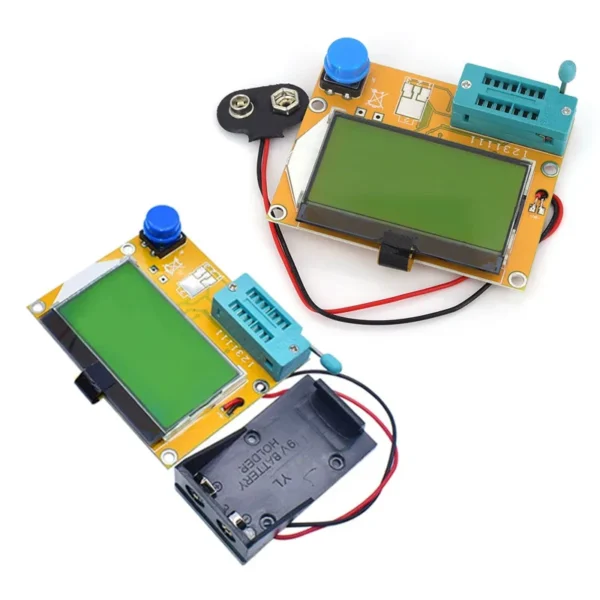 LCR-T4 T3 ESR Meter Transistor Tester Diode Triode Capacitance SCR Inductance MOS PNP NPN
$1.90 – $8.90Price range: $1.90 through $8.90
LCR-T4 T3 ESR Meter Transistor Tester Diode Triode Capacitance SCR Inductance MOS PNP NPN
$1.90 – $8.90Price range: $1.90 through $8.90
 AI Robot Echo Ear Learning Education AI Assistant Chatbot Emotional Interactive Companion Gift For Children
$52.80
AI Robot Echo Ear Learning Education AI Assistant Chatbot Emotional Interactive Companion Gift For Children
$52.80
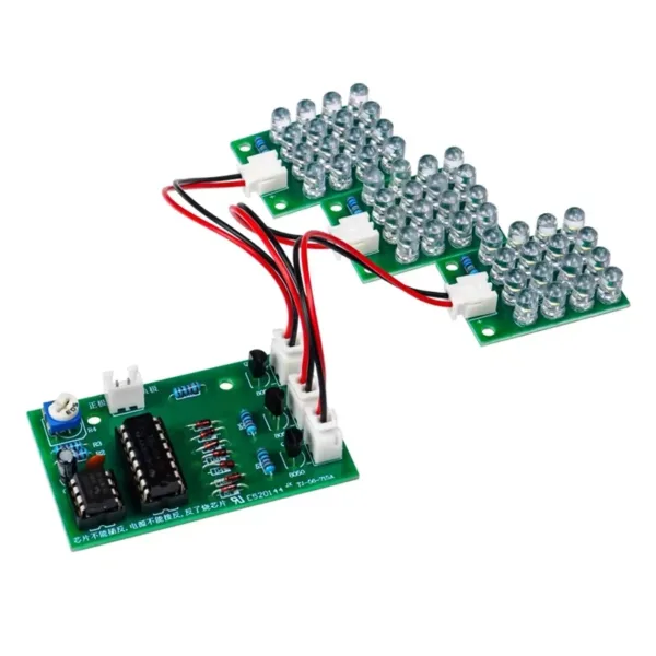 DIY Electronic Welding Practice Kit NE555 Red, White And Blue Flash LED Alarm Light Strobe Module Production Design Kit
$6.90
DIY Electronic Welding Practice Kit NE555 Red, White And Blue Flash LED Alarm Light Strobe Module Production Design Kit
$6.90
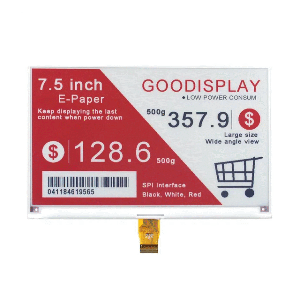 7.5inch E-Paper Red Electronic Paper Display Tri-color E-ink Display 1.3s Partial Update of Black and White Parts
$46.90 – $68.90Price range: $46.90 through $68.90
7.5inch E-Paper Red Electronic Paper Display Tri-color E-ink Display 1.3s Partial Update of Black and White Parts
$46.90 – $68.90Price range: $46.90 through $68.90
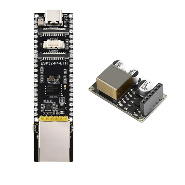 ABMF-ESP32-P4-ETH Development Board RJ45 Ethernet Port MIPI-DSI Interface 40PIN GPIO 32MB PSRAM For AI Deepseek Support With POE
$18.90
ABMF-ESP32-P4-ETH Development Board RJ45 Ethernet Port MIPI-DSI Interface 40PIN GPIO 32MB PSRAM For AI Deepseek Support With POE
$18.90