When hardware engineers review a Gerber file, they often obsess over trace impedance and component placement. Yet, the most catastrophic field failures and SMT yield killers frequently originate from a single, overlooked feature: the PCB via.
Vias are the vertical highways of a printed circuit board. However, treating them as simple "connect-the-dots" holes is a critical mistake. Poor via design leads to solder wicking during reflow, trapped chemicals causing long-term corrosion, and signal reflection in high-speed digital circuits.
This guide bypasses basic textbook definitions. We will dissect the real-world manufacturing constraints of PCB drilling, expose the hidden reliability risks of via protection methods, and provide the strict Design for Manufacturability (DFM) rules you need to master High-Density Interconnect (HDI) and Via-in-Pad technologies.
The Anatomy of PCB Vias: Beyond Basic Through-Holes
To design for reliability, you must first understand the functional classification of holes in a PCB stack-up.
1. Plated vs. Non-Plated Holes
- PTH (Plated Through-Hole): The barrel of the hole is metallized via electroless copper deposition, creating an electrical connection between layers.
- NPTH (Non-Plated Through-Hole): Dry holes used strictly for mechanical mounting, alignment, or heat dissipation. They carry no electrical current.
2. Layer Interconnect Vias
- Through-Hole Vias: Drilled completely through the entire board stack-up. The most cost-effective but consumes routing space on all layers.
- Blind Vias: Connect an outer layer to one or more adjacent inner layers. Essential for HDI designs, allowing dense routing on the surface without wasting inner layer space.
- Buried Vias: Connect only inner layers and are completely invisible from the outside. Highly expensive due to the sequential lamination process required, but maximizes internal routing density.
3. High-Speed Signal Integrity Vias
- Back-Drilling: In high-speed digital designs (e.g., PCIe, DDR4/5), the unused portion of a through-hole via acts as an antenna stub, causing severe signal reflection and EMI. Back-drilling removes this "stub" from the bottom of the board, preserving signal integrity up to multi-gigahertz frequencies.
The Hidden Nightmare: Why "Tented Vias" Fail in Mass Production
One of the most common DFM mistakes is relying on via tenting (covering the via annular ring with solder mask) for protection in mass-production boards.
While tenting is cheap and acceptable for simple 2-layer prototypes, it is a massive liability for high-reliability or multi-layer boards. Here is the manufacturing reality:
- The Outgassing Explosion: During the reflow soldering process (peaking at 260°C), moisture and trapped air inside the tented via expand rapidly. This pressure frequently blows the solder mask off the via, creating a "blister" that ruins the board's aesthetics and exposes the copper to oxidation.
- Chemical & Solder Trapping: Solder mask is not a perfect seal. During the PCB fabrication process, etching chemicals or plating solutions can seep into the via and become trapped. Later, during wave soldering, liquid solder can wick into the via, creating hidden solder balls that eventually break loose and cause intermittent short circuits.
The Engineering Verdict: Never specify tented vias for boards undergoing lead-free reflow or operating in harsh environments.
Via Plugging Methods: Epoxy vs. Ink – Choosing the Right Reliability
If tenting is a risk, the via must be plugged. The industry primarily uses two methods, and choosing the wrong one will compromise your SMT yield.
1. Ink Plugging (Solder Mask Filled)
This process forces UV-curable solder mask into the via.
- Pros: Low cost, provides basic insulation.
- Cons: Solder mask has a high Coefficient of Thermal Expansion (CTE) compared to the FR-4 substrate. During thermal cycling, the ink expands at a different rate than the board, leading to "ink outgassing" or cracking at the via mouth. It also leaves a slight dimple on the surface, making it unsuitable for fine-pitch components.
2. Epoxy Filling (Resin Plugged)
This process injects specialized, thermally conductive epoxy resin into the via, which is then cured and planarized (ground flat).
- Pros: The CTE of the epoxy is closely matched to the FR-4 substrate, eliminating thermal expansion cracks. It creates a hermetic seal, preventing chemical entrapment and solder wicking. The surface is perfectly flat after planarization.
- Cons: Higher manufacturing cost and longer lead times.
The Engineering Verdict: For any board containing BGA components, fine-pitch QFNs, or requiring IPC Class 3 reliability, epoxy-filled vias are mandatory.
Via-in-Pad (VIP) Technology: The Secret to Ultra-High-Density HDI
As component packages shrink (e.g., 0.4mm pitch BGAs), there is physically no space to route traces out of the pads using traditional "dog-bone" fanout patterns. The solution is Via-in-Pad Plated Over (VIPPO).
VIP technology places the via directly inside the component's solder pad. To prevent the solder paste from flowing down the via during reflow (which causes cold joints or tombstoning), the via must be meticulously processed:
- Drill & Plate: The via is drilled and initially plated.
- Epoxy Fill: The via is completely filled with conductive or non-conductive epoxy.
- Cure & Planarize: The epoxy is baked and ground perfectly flat with the surrounding copper layer.
- Plate Over & Surface Finish: A layer of copper is plated over the filled via, followed by the final surface finish (ENIG or ENEPIG).
Critical VIP Design Rules for DFM:
- Via Size: The finished hole diameter should ideally be between 0.15mm and 0.30mm. Vias larger than 0.3mm are difficult to fill completely without voids.
- Annular Ring: Ensure a minimum annular ring of 0.10mm to 0.15mm around the via to prevent drill breakout.
- Clearance: Maintain strict clearance between the via-in-pad and adjacent high-speed traces to prevent impedance discontinuities.
Mechanical Drilling Constraints: What the Factory Floor Actually Sees
Designers often assume CNC machines can drill any size hole anywhere. The physical reality of mechanical drilling imposes strict limitations.
- Drill Bit Increments: Standard carbide drill bits are manufactured in 0.05mm increments. If you design a 0.23mm hole, the manufacturer will round it to the nearest available bit (0.20mm or 0.25mm). Always design your hole sizes to match standard increments to avoid delays.
- Aspect Ratio (Thickness-to-Diameter): This is the ultimate bottleneck. The industry standard maximum aspect ratio for mechanical drilling is typically 10:1. If your board is 1.6mm thick, the smallest reliable drill bit you can use is 0.16mm. Pushing beyond 10:1 risks drill bit breakage and poor desmear (inadequate cleaning of the hole wall), leading to via barrel cracks.
- Hole-to-Hole Spacing: Maintain a minimum distance of 0.15mm to 0.20mm between the edges of adjacent drill hits. Insufficient spacing can cause the fiberglass weave to tear during drilling, resulting in a catastrophic short.
The Startup Advantage: Rapid Via Validation Without Financial Risk
Designing complex HDI boards with blind vias, back-drilling, or Via-in-Pad requires rigorous physical validation. You cannot rely solely on 2D simulations; you must test the actual thermal relief, solder paste printing, and BGA placement on physical hardware. Iterating through multiple prototype spins to perfect your via design can rapidly drain a startup's R&D budget.
This is not a gimmick; it is a strategic engineering tool. It allows you to:
- Validate Mechanical Fit: Test the physical breakaway of mouse bites or the clearance of edge connectors.
- Iterate Fearlessly: Test different via tenting, plugging, or VIP designs on a test coupon without financial penalty.
- Accelerate R&D: Order multiple layout variants simultaneously to compare real-world SMT assembly results.
Scaling Your Design: From DFM to Turnkey Mass Production
Once your via design is validated and your prototype passes thermal cycling, the focus shifts to scalable assembly. A flawless via design can still be ruined by poor solder paste volume, misaligned stencils, or counterfeit components during the PCBA phase.
Transitioning from a validated prototype to mass production requires a partner who understands the intricate relationship between bare board fabrication and SMT assembly. By utilizing our turnkey PCB prototype and assembly manufacturing services, you ensure that the CAM engineers reviewing your Gerber files are the same experts managing your SMT lines. They will optimize your stencil apertures specifically for your via-in-pad design, guaranteeing perfect solder paste deposition and eliminating cold joints.
If you are preparing to scale your product line and need to optimize panelization, secure component allocation, and drive down per-unit costs, initiating an OEM/ODM bulk manufacturing inquiry early in your design cycle allows our engineering team to align your BOM and layout with the most cost-effective mass-production methodologies.
FAQ
Q: What is the difference between via tenting and via plugging?
A: Via tenting simply covers the via annular ring with solder mask, leaving the hole hollow. Via plugging physically fills the hole with ink or epoxy. Plugging prevents solder wicking and chemical entrapment, making it mandatory for high-reliability and BGA designs.
Q: Why is my manufacturer rejecting my 0.1mm via on a 1.6mm thick board?
A: This violates the aspect ratio rule. A 0.1mm hole in a 1.6mm board has a 16:1 aspect ratio, which exceeds the standard 10:1 mechanical drilling limit. The drill bit will likely snap, or the plating inside the hole will be too thin and unreliable. You must either reduce the board thickness, increase the via size, or use laser-drilled blind vias.
Q: Can I use via-in-pad for through-hole components?
A: No. Via-in-pad is strictly for Surface Mount Technology (SMT) pads. Through-hole components require the physical lead to pass through the board for mechanical strength and wave soldering. Plugging a via under a through-hole pad defeats the purpose of the mechanical interlock.
Q: How do you ensure the epoxy in a via-in-pad doesn't crack during reflow?
A: We use high-Tg, low-CTE (Coefficient of Thermal Expansion) epoxy resins specifically formulated to match the expansion rate of the FR-4 substrate. Combined with a strict, controlled reflow profile, this eliminates the thermal stress that causes cracking.
Stop Letting Poor Via Design Dictate Your Yield
Mastering PCB drilling and via design is the difference between a board that works on a screen and a product that survives in the field. By understanding the physical realities of aspect ratios, epoxy plugging, and Via-in-Pad processing, you can design boards that are not only electrically brilliant but also highly manufacturable.
Whether you are utilizing our $2 for 5 pieces (under 50x50mm) offer to validate your latest HDI layout, or you are ready to scale a complex, multi-layer design into high-volume production, our engineering team is prepared to provide the actionable DFM feedback and precision manufacturing your project demands.
Ready to build with confidence?
Reach out to our engineering team today for a comprehensive DFM review of your via design and a precise manufacturing quote. Let's engineer a product that is as robust in manufacturing as it is in design.

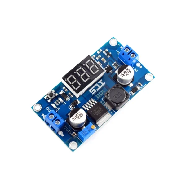 Upgraded Version XL6009 Boost Module DC-DC 5V-32V To 5V-40V 4A Adjustable Step Up Power Supply Module with Digital Display
$3.50
Upgraded Version XL6009 Boost Module DC-DC 5V-32V To 5V-40V 4A Adjustable Step Up Power Supply Module with Digital Display
$3.50
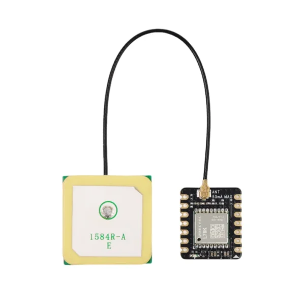 GNSS add on Module for Seeed Studio XIAO - UART Interface, mini GPS/Tracker, Powered by Quectel L76K
$18.90
GNSS add on Module for Seeed Studio XIAO - UART Interface, mini GPS/Tracker, Powered by Quectel L76K
$18.90
 Radxa PD 30W Power Adapter SBC Supports 5V/5A
$14.99
Radxa PD 30W Power Adapter SBC Supports 5V/5A
$14.99
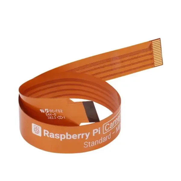 Raspberry Pi 5 FPC Adapter Cable - 22-Pin to 15-Pin DSI/CSI Cable for Official Display or Camera (200mm or 300mm)
$8.30
Raspberry Pi 5 FPC Adapter Cable - 22-Pin to 15-Pin DSI/CSI Cable for Official Display or Camera (200mm or 300mm)
$8.30
 Dynamic CM4 Expansion Board 2.8inch Touch Screen Display HAT USB HUB Starter Kit for RPI Raspberry Pi Compute Module 4 Lite EMMC
$66.90
Dynamic CM4 Expansion Board 2.8inch Touch Screen Display HAT USB HUB Starter Kit for RPI Raspberry Pi Compute Module 4 Lite EMMC
$66.90