You have built a brilliant ESP32-based IoT product. The firmware is rock-solid. The industrial design is award-worthy. You book a $5,000 slot at an accredited EMC/RF testing lab, ship your "Golden Samples," and wait two weeks for the results.
Then the email arrives: FAIL.
Your device exceeded the radiated emissions limit at 2.4 GHz by 3dB. Or worse, the conducted emissions on the power rail are out of spec. The lab engineer's report is filled with phrases like "inconsistent solder joint quality on RF ground vias" and "shielding enclosure not making reliable contact with PCB ground pads."
You just burned $5,000 on a failed test, and the re-test will cost another $3,000 plus weeks of delay. Your Amazon launch date slips. Your Kickstarter backers get angry. Investors get nervous.
Here is the truth that most hardware startups discover too late: FCC/CE certification failure is rarely a design problem. It is a manufacturing consistency problem.
At esp32s.com, we have helped dozens of IoT companies achieve first-pass FCC/CE certification for their ESP32-based products. In this guide, we will reveal the specific PCBA manufacturing variables that directly determine whether your device passes or fails RF and EMC testing—and exactly how our quality-controlled turnkey assembly process eliminates these risks.
Why RF Certification is a Manufacturing Challenge, Not Just a Design Challenge
Engineers often assume that if their schematic is correct and their PCB layout follows Espressif's reference design, certification will be straightforward. This assumption ignores a fundamental reality:
Certification labs do not test your schematic. They test your physical, manufactured board.
And no two manufactured boards are identical. Variations in solder joint geometry, component placement accuracy, ground plane continuity, and shielding contact pressure all introduce parasitic inductances and capacitances that can shift your RF emissions profile by several dB—enough to cross the regulatory limit.
When you build 5 prototype boards by hand or through a low-quality assembly house, they might pass. But when you build 500 units for mass production, statistical variation means some units will fail. FCC certification requires you to test production-representative units, and a single outlier can fail the entire product family.
The 5 PCBA Manufacturing Variables That Make or Break FCC/CE Certification
Variable 1: RF Ground Via Solder Fill Consistency
The Physics: Your ESP32 PCB design likely includes an array of ground vias (a "via fence") surrounding the RF section and antenna feedline. These vias are meant to create a Faraday cage, preventing the 2.4 GHz signal from radiating into unintended areas of the board.
The Manufacturing Risk: In a reflow process, solder paste must wick down through these vias to create a solid copper-to-copper connection between all layers. If the via is too large relative to the pad, or if the reflow temperature profile is insufficient, the solder may not fully fill the via. This creates a high-impedance ground path at 2.4 GHz, effectively breaking the Faraday cage and allowing RF energy to leak.
- We perform X-Ray Inspection on a statistically significant sample of every production run, specifically targeting RF ground vias to verify 100% solder fill.
- We optimize the stencil aperture ratio for via-in-pad designs to ensure sufficient solder volume without causing solder balling.
- If your design uses tented vias (covered by solder mask), we flag this during DFM review, as tented vias cannot be reliably soldered and should be replaced with filled-and-capped vias for RF-critical applications.
Variable 2: ESP32 Module Shield Grounding
The Physics: The metal shield (can) over the ESP32-WROOM or WROVER module is not just for protection. It is a critical RF ground reference. The shield must make low-impedance electrical contact with the PCB ground plane at multiple points around its perimeter.
The Manufacturing Risk: The shield connects to the PCB through a series of small SMD pads around the module's edge. If the solder paste volume on these pads is insufficient, or if the reflow profile causes the module to "float" slightly during melting (due to surface tension imbalance), the shield may make contact at only 3 out of 8 ground pads. This creates an asymmetric ground path, causing the shield itself to act as a parasitic antenna, radiating harmonics that fail FCC radiated emissions tests.
- We use 3D Solder Paste Inspection (SPI) before component placement to verify that the solder paste volume on every shield ground pad is within ±10% of the target. This prevents both insufficient paste (open circuits) and excess paste (short circuits).
- We monitor the reflow oven's soak zone dwell time to ensure the ESP32 module's large thermal mass reaches proper temperature without causing thermal gradients that shift the module during the liquidus phase.
Variable 3: Crystal Oscillator Parasitic EMI
The Physics: The 40 MHz crystal oscillator is the heartbeat of the ESP32. Its fundamental frequency and harmonics (80 MHz, 120 MHz, 160 MHz, etc.) are among the most common sources of radiated and conducted emissions failures in FCC testing.
The Manufacturing Risk: If the load capacitors (typically 2 x 10-15pF) placed next to the crystal have poor solder joints (cold joints, tombstoning, or insufficient wetting), the oscillator circuit's impedance changes. This can cause:
- Frequency drift outside the crystal's specified tolerance.
- Increased harmonic content (the waveform becomes less sinusoidal and more distorted, generating stronger harmonics).
- These harmonics can radiate through PCB traces and cables, causing broadband emissions failures.
- Crystal oscillators and their load capacitors are classified as Critical Components in our assembly process. They receive enhanced AOI inspection with stricter acceptance criteria.
- We verify the solder joint fillet shape on both pads of every crystal load capacitor, ensuring a concave meniscus that indicates proper wetting.
Variable 4: Power Plane Decoupling & Switching Noise
The Physics: The ESP32's Wi-Fi transmitter draws up to 500mA in rapid bursts. If the power delivery network (PDN) on your PCB has high impedance at certain frequencies, these current bursts create voltage ripple that couples into the RF signal chain, generating spurious emissions (unwanted signals at frequencies outside the intended Wi-Fi channel).
The Manufacturing Risk: If the bulk decoupling capacitors (10µF, 100µF) have ESR (Equivalent Series Resistance) variations due to poor soldering or component batch inconsistency, the PDN impedance profile changes from board to board. A board with a marginal PDN might pass FCC on a quiet day but fail when the Wi-Fi duty cycle increases.
- We source decoupling capacitors from a single, locked lot for each production run to minimize batch-to-batch ESR variation.
- For high-volume runs, we can perform PDN impedance measurements using a Vector Network Analyzer (VNA) on sample boards, verifying that the manufactured PDN matches the simulated impedance profile from your design tool.
Variable 5: Cable & Connector Shield Termination
The Physics: If your ESP32 device has external cables (USB, power, antenna extension), these cables act as unintentional antennas for any common-mode noise on the PCB. FCC testing specifically measures emissions from attached cables.
The Manufacturing Risk: The connector's metal shell must be soldered to the PCB ground plane with zero impedance. If the through-hole or SMT connector has incomplete solder fillets on its shield/ground tabs, the cable shield is not properly terminated. This creates a common-mode antenna that radiates the ESP32's digital switching noise, causing broadband emissions failures from 30 MHz to 1 GHz.
- All connector shield tabs are inspected via 3D AOI with a specific pass/fail criterion for solder fillet height and coverage.
- For through-hole connectors with large thermal mass ground tabs, we use selective wave soldering or extended reflow profiles to ensure complete wetting, even on 4-layer boards with heavy internal ground planes that act as heat sinks.
The "Golden Sample" Trap: Why Your Prototypes Pass but Production Fails
This is the most dangerous scenario in IoT manufacturing:
- You hand-solder or use a hobbyist assembly house to build 5 prototype boards.
- You carefully select the best-performing board as your "Golden Sample."
- You submit this Golden Sample to the FCC lab, and it passes.
- You celebrate, order 1,000 units from a volume manufacturer, and ship to customers.
- Customers report intermittent Wi-Fi disconnections. An independent lab test reveals that 15% of production units exceed FCC emissions limits.
- You face a forced recall, regulatory fines, and destroyed brand reputation.
This happens because the Golden Sample was a statistical outlier. Its solder joints happened to be perfect, its ground vias happened to be fully filled, and its crystal happened to oscillate cleanly. But the manufacturing process that produced it was not controlled, not inspected, and not repeatable.
FCC/CE certification is not about making one perfect board. It is about making ten thousand identical boards.
The esp32s.com Certification-Ready Manufacturing System
When you partner with us for your ESP32 product's turnkey PCBA, you are not just buying assembly labor. You are buying a certification-ready quality system:
- Pre-Certification DFM Audit: Before production, our engineers review your PCB layout specifically for FCC/CE risk factors: via fence density, shield pad count, connector grounding, and filter component placement.
- Statistical Process Control (SPC): We monitor solder paste volume (SPI), placement accuracy (PNP), and solder joint quality (AOI/X-Ray) using real-time SPC charts. If any parameter drifts toward the control limit, the line is stopped and corrected before defects are produced.
- RF Consistency Testing: For production runs, we can implement a basic conducted RF power test using a spectrum analyzer to verify that every unit's Wi-Fi output power and harmonic content fall within a tight tolerance band. Units outside the band are rejected before shipping.
- Full Traceability: Every board we ship has a unique serial number linked to its component lot numbers, SPI data, AOI images, and test results. If a certification issue arises, we can trace it to the exact batch and process step.
The Financial Case: Quality PCBA vs. Certification Failure
Let's compare the economics of investing in quality manufacturing versus absorbing a certification failure:
The math is clear: investing in a PCBA partner with certification-grade quality control is the cheapest insurance policy you can buy for your IoT product launch.
Ready to Certify with Confidence?
Don't gamble your product launch on inconsistent manufacturing. Let esp32s.com build your ESP32 boards with the precision, inspection, and traceability that FCC/CE certification demands.
Upload your Gerber files and BOM today, and request our Certification-Ready DFM Audit alongside your turnkey quote.
Frequently Asked Questions (FAQ)
Q: Can you guarantee that my ESP32 product will pass FCC/CE certification?
A: No PCBA manufacturer can guarantee certification, as the outcome depends on the overall product design (enclosure, cable routing, firmware power management). However, we can guarantee that our manufacturing process will not introduce variability that causes failure. Our certification-ready DFM audit identifies and eliminates the most common manufacturing-related causes of RF/EMC test failure.
Q: Do you perform pre-compliance EMC testing in-house?
A: We offer basic conducted and radiated emission screening using spectrum analyzers and near-field probes as part of our functional testing services. This can identify major issues before you spend money on a full anechoic chamber test at an accredited lab. For formal pre-compliance or certification testing, we recommend and can coordinate with accredited third-party EMC labs.
Q: How does your X-Ray inspection help with RF certification?
A: X-Ray inspection verifies the internal solder quality of components that optical cameras cannot see—specifically the ESP32 module's hidden ground pads, RF ground vias, and BGA/QFN components. Poor solder joints on these connections create high-impedance ground paths that directly cause radiated emissions failures. X-Ray ensures every critical RF ground connection is solid.
Q: What is the minimum order quantity for certification-grade PCBA?
A: Our certification-grade quality protocols (SPI, 3D AOI, X-Ray, SPC) are applied to every production run, regardless of quantity. Whether you need 50 units for FCC testing or 5,000 units for market launch, every board receives the same rigorous inspection and traceability.

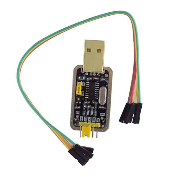 CH340 Module Instead of PL2303 CH340G CH340E RS232 to TTL Module Upgrade USB to Serial Port In Nine Brush Plate For Arduino
$2.90
CH340 Module Instead of PL2303 CH340G CH340E RS232 to TTL Module Upgrade USB to Serial Port In Nine Brush Plate For Arduino
$2.90
 Excellent Esp32-Aduio-Kit Wifi+ Bluetooth Module Esp32 Serial To Wifi / Esp32-Aduio-Kit Audio Development Board With Esp32-A1S
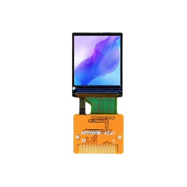 0.6" Inch Small Size IPS TFT Color Screen 128x150 SPI Interface with ST7735P3 Full View Display Module 12P Pins
$3.20
0.6" Inch Small Size IPS TFT Color Screen 128x150 SPI Interface with ST7735P3 Full View Display Module 12P Pins
$3.20
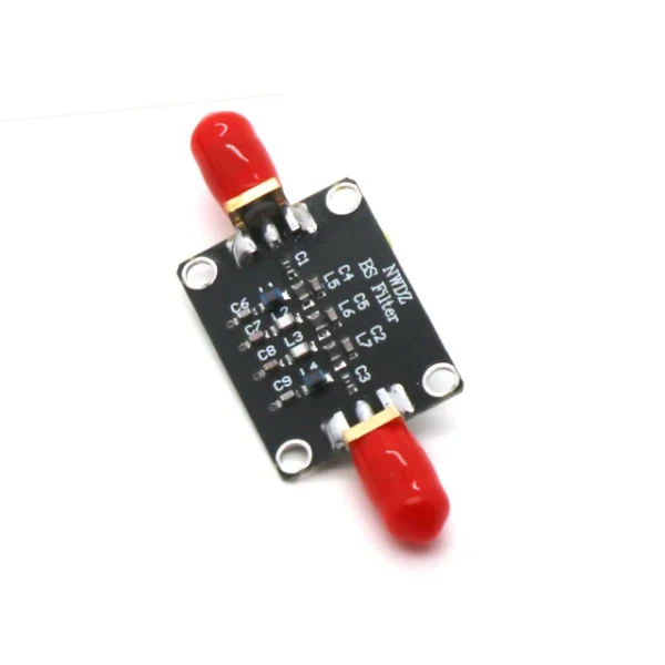 88-108Mhz FM Bandstop Filter FM Band Stop Filter Passive Notch For Radio Amplifier Anti-FM Interference Rtl-sdr Blog Shortwave
$5.90
88-108Mhz FM Bandstop Filter FM Band Stop Filter Passive Notch For Radio Amplifier Anti-FM Interference Rtl-sdr Blog Shortwave
$5.90
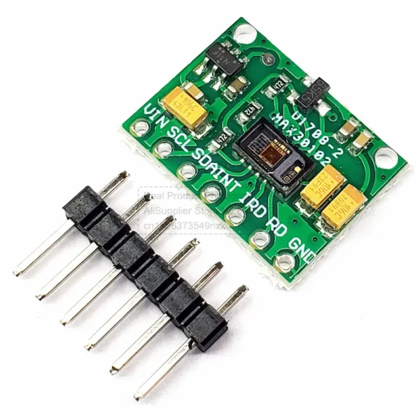 MAX30102 Blood Oxygen Heart Rate Sensor Pulse Heartbeat Oxygen Concentration Sensor for Arduino Replace MAX30100